
TPS62730DRYR (1)
Manufacturer Part Number
TPS62730DRYR
Manufacturer
Texas Instruments
Introduction
The TPS62730DRYR is a step-down converter designed specifically for power management in applications like Bluetooth products. It is engineered to provide efficient power management and extend battery life in portable devices.
Product Features and Performance
High-efficiency step-down converter
Supports input voltages from 1.9V to 3.9V
Delivers a stable output voltage of 2.1V
Ensures stable operation across -40°C to 85°C
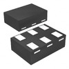
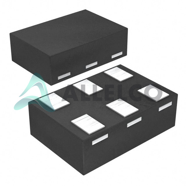
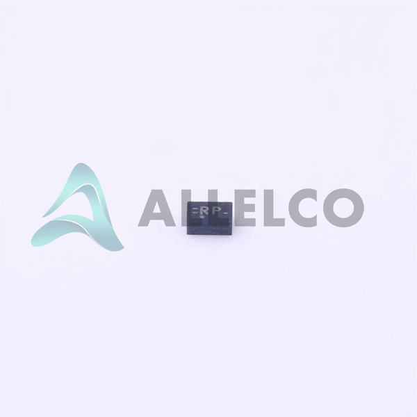
Compact 6-UFDFN package for space-sensitive applications
Integrated power-saving features for extended battery life
Product Advantages
Exceptionally low quiescent current enhances battery life
Highly efficient conversion minimizes thermal footprint
Designed for easy integration in compact devices
Robust temperature range ensures performance in varied environments
TPS62730DRYR (2)
Key Technical Parameters
Voltage Input: 1.9V ~ 3.9V
Voltage Output: 2.1V
Operating Temperature: -40°C ~ 85°C
Package / Case: 6-UFDFN
Supplier Device Package: 6-SON (1.45x1)
Quality and Safety Features
Built with protective features against overcurrent and thermal overload
Manufactured following stringent quality standards of Texas Instruments
Compatibility
Ideal for Bluetooth applications and compatible with a wide range of portable devices
Application Areas
Power management for Bluetooth devices
Wearable technology
Portable electronics including medical devices and smart sensors
Product Lifecycle
Currently active with no immediate discontinuation forecast
Continuous support and availability of upgrades from Texas Instruments
Several Key Reasons to Choose This Product
High-efficiency design reduces power consumption and extends battery life
Compact and lightweight, ideal for space-constrained applications
Supports a wide operating temperature range, suitable for a variety of environments
Texas Instruments is renowned for its reliability and quality in power management technology
Ongoing product support and availability ensure a sound investment


 TPS62701YZFTTexas InstrumentsIC REG BUCK PROG 650MA 8DSBGA
 TPS62736RGYRTexas InstrumentsIC REG BUCK PROG 50MA 14VQFN
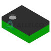 TPS62697YFFTTexas Instruments4-MHZ HIGH-EFFICIENCY STE-DOWN C
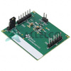 TPS62733EVM-726Texas InstrumentsEVAL MODULE FOR TPS62733-726
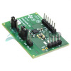 TPS62736EVM-205Texas InstrumentsEVALUATION BOARD FOR TPS62736
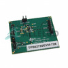 TPS62730EVM-726Texas InstrumentsEVAL MODULE FOR TPS62730
 TPS62693YFDTTexas InstrumentsIC REG BUCK 2.85V 800MA 6DSBGA
 TPS62730DRYTexas Instruments


