

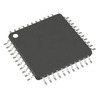
 ATMEGA8535L-8AIAtmelIC MCU 8BIT 8KB FLASH 44TQFP
 ATMEGA8535L-8MURAtmelIC MCU 8BIT 8KB FLASH 44VQFN
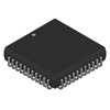
 ATMEGA8535L-8JUMicrochip TechnologyIC MCU 8BIT 8KB FLASH 44PLCC
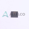 ATMEGA8535L-8MUMicrochip TechnologyIC MCU 8BIT 8KB FLASH 44VQFN
 ATMEGA8535L-8JCAtmel
- Dani***alkerTech
- Jun 1, 2026

Image may be representation.
See specifications for product details.
See specifications for product details.
- EXPRESS OPTION
- Payment method
ATMEGA8535L-8JJ - Microchip Technology
- Manufacturer Part Number
- ATMEGA8535L-8JJ
- Manufacturer
- Microchip Technology
- Allelco Part Number
- 98D-ATMEGA8535L-8JJ
- Warranty
- 1 Year Allelco Warranty - Find out more
- Stock Status:
- 7,326 pcs available, New & Original
- Parts Description
- IC MCU 8BIT 8KB FLASH 44PLCC
- Package
- 44-PLCC (16.6x16.6)
- Data sheet
-
ATMEGA8535L-8JJ.pdf
Datasheets
ATMEGA8535(L) Complete.pdfHTML Datasheet
Cylindrical Battery Holders.pdf
- RoHs Status
- ROHS3 Compliant
- Our certification
- In stock: 7326


