View All

Please refer to the English Version as our Official Version.Return

Europe
France(Français) Germany(Deutsch) Italy(Italia) Russian(русский) Poland(polski) Czech(Čeština) Luxembourg(Lëtzebuergesch) Netherlands(Nederland) Iceland(íslenska) Hungarian(Magyarország) Spain(español) Portugal(Português) Turkey(Türk dili) Bulgaria(Български език) Ukraine(Україна) Greece(Ελλάδα) Israel(עִבְרִית) Sweden(Svenska) Finland(Svenska) Finland(Suomi) Romania(românesc) Moldova(românesc) Slovakia(Slovenská) Denmark(Dansk) Slovenia(Slovenija) Slovenia(Hrvatska) Croatia(Hrvatska) Serbia(Hrvatska) Montenegro(Hrvatska) Bosnia and Herzegovina(Hrvatska) Lithuania(lietuvių) Spain(Português) Switzerland(Deutsch) United Kingdom(English)
Asia/Pacific
Japan(日本語) Korea(한국의) Thailand(ภาษาไทย) Malaysia(Melayu) Singapore(Melayu) Vietnam(Tiếng Việt) Philippines(Pilipino)
Africa, India and Middle East
United Arab Emirates(العربية) Iran(فارسی) Tajikistan(فارسی) India(हिंदी) Madagascar(malaɡasʲ)
South America / Oceania
New Zealand(Maori) Brazil(Português) Angola(Português) Mozambique(Português)
North America
United States(English) Canada(English) Haiti(Ayiti) Mexico(español)
HomeProductsIntegrated Circuits (ICs)Embedded - MicrocontrollersR5F100FCAFP#30
R5F100FCAFP#30 Image
Image may be representation.
See specifications for product details.
EXPRESS OPTION
Payment method

R5F100FCAFP#30 - Renesas Electronics America Inc

Manufacturer Part Number
R5F100FCAFP#30
Manufacturer
Renesas Electronics Corporation
Allelco Part Number
32D-R5F100FCAFP#30
Warranty
1 Year Allelco Warranty - Find out more
Stock Status:
30,045 pcs available, New & Original
Parts Description
IC MCU 16BIT 32KB FLASH 44LQFP
Package
44-LQFP (10x10)
Data sheet
R5F100FCAFP#30.pdf
RoHs Status
ROHS3 Compliant
Our certification
In stock: 30045
  • Unit Price: $0.773
  • Subtotal: $0.00

Want a better price?
Add to Cart and Submit RFQ now, we'll contact you immediately.

Quantity Unit Price Ext. Price
1+ $0.773 $0.77
200+ $0.30 $60.00
500+ $0.289 $144.50
1000+ $0.284 $284.00
The above prices does not include taxes and freight rates, which will be calculated on the order pages.

Specifications

R5F100FCAFP#30 Tech Specifications
Renesas Electronics America Inc - R5F100FCAFP#30 technical specifications, attributes, parameters and parts with similar specifications to Renesas Electronics America Inc - R5F100FCAFP#30

Product Attribute Attribute Value
Manufacturer Renesas Electronics Corporation
Voltage - Supply (Vcc/Vdd) 1.6V ~ 5.5V
Supplier Device Package 44-LQFP (10x10)
Speed 32MHz
Series RL78/G13
RAM Size 2K x 8
Program Memory Type FLASH
Program Memory Size 32KB (32K x 8)
Peripherals DMA, LVD, POR, PWM, WDT
Package / Case 44-LQFP
Package Tray
Product Attribute Attribute Value
Oscillator Type Internal
Operating Temperature -40°C ~ 85°C (TA)
Number of I/O 31
Mounting Type Surface Mount
EEPROM Size 4K x 8
Data Converters A/D 10x8/10b
Core Size 16-Bit
Core Processor RL78
Connectivity CSI, I²C, LINbus, UART/USART
Base Product Number R5F100

Environmental & Export Classifications

ATTRIBUTE DESCRIPTION
RoHs Status ROHS3 Compliant
Moisture Sensitivity Level (MSL) 3 (168 Hours)
REACH Status REACH Unaffected
ECCN 3A991A2
HTSUS 8542.31.0001

Parts Introduction

R5F100FCAFP#30 Image
R5F100FCAFP#30 (1)

Manufacturer Part Number

R5F100FCAFP#30

Manufacturer

Renesas Electronics America

Introduction

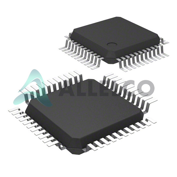
The R5F100FCAFP#30 is a cutting-edge 16-Bit microcontroller from Renesas Electronics America, designed for embedded applications demanding high performance and low power consumption. It belongs to the RL78/G13 series and comes in a 44-LQFP packaging.

Product Features and Performance

Core Processor: RL78, offering robust performance with a 16-bit architecture

Speed: Operates at a maximum frequency of 32MHz, ensuring swift processing capabilities

Connectivity Options: Includes CSI, I2C, LINbus, UART/USART for versatile peripheral connections

Integrated Peripherals: Features DMA, LVD, POR, PWM, WDT for enhanced functionality

Program Memory: 32KB of FLASH memory facilitating complex applications

EEPROM Size: 4K x 8, providing ample space for data that must be retained across reboots

RAM: 2K x 8, ensuring sufficient temporary data storage for operations

Voltage Range: 1.6V to 5.5V, supporting a variety of power supply configurations

Product Advantages

Low Power Consumption: Designed for energy-efficient operation, extending battery life in portable devices

High Integration: Combines multiple functionalities reducing the need for external components

Flexible Connectivity: Supports a broad range of communication protocols for easy integration with other devices

Enhanced Safety Features: Includes LVD and POR for system reliability

Key Technical Parameters

Core Size: 16-Bit

Number of I/O: 31

Data Converters: A/D 10x8/10b, for accurate analog to digital conversions

Oscillator Type: Internal, simplifying system design

Operating Temperature: -40°C to 85°C, suited for harsh environments

Quality and Safety Features

Built-in Watchdog Timer (WDT) to prevent system malfunctions

Low Voltage Detection (LVD) ensures the microcontroller operates within safe voltage levels

Compatibility

Compatible with a range of development tools and software provided by Renesas, facilitating rapid development and deployment

Application Areas

Ideal for automotive applications, industrial control systems, home appliances, and consumer electronics

Product Lifecycle

Status: Active, indicating that the product is widely available and not nearing discontinuation

Renesas provides ongoing support, with potential future upgrades to enhance functionalities

Several Key Reasons to Choose This Product

High Performance: The 32MHz operating frequency enables demanding applications to run smoothly

Energy Efficiency: Optimized for low power consumption, making it ideal for battery-powered devices

Broad Connectivity: Multiple communication interfaces offer flexibility in system design

Robust Peripheral Set: Integrated peripherals minimize additional component requirements, simplifying design and reducing overall cost

Reliable Operation: Quality and safety features ensure stable operation in various conditions

Strong Support and Longevity: Supported by Renesas with a commitment to long-term availability and support

Frequently Asked Questions(FAQ)

How does the R5F100FCAFP#30 compare to other RL78/G13 microcontrollers in terms of power efficiency and peripheral integration for battery-powered IoT sensor nodes operating at 2.4V?
The R5F100FCAFP#30 offers a balanced combination of low-voltage operation down to 1.6V and moderate peripheral integration, making it suitable for extended battery life in constrained environments. While its 32KB flash and 2KB RAM are adequate for simple sensing tasks, it lacks advanced power-saving modes found in newer RL78 variants such as the G14 series with integrated LCD drivers or ultra-low-power sleep currents below 1µA. Its 10-bit ADC with eight channels supports typical analog sensor readings, but applications requiring higher resolution or faster sampling may need external ADCs. The inclusion of LINbus and I2C peripherals enables flexible communication with legacy sensors and short-range networks, though Wi-Fi or BLE connectivity would require external modules.
What is the maximum number of GPIOs available on the R5F100FCAFP#30 when using alternate function multiplexing, and how does this affect real-time control of motor-driven systems?
The R5F100FCAFP#30 provides 31 general-purpose I/O pins, all of which can be reassigned through alternate function mapping depending on active peripherals like UART, I2C, or PWM outputs. However, simultaneous use of high-demand peripherals—such as multiple PWM channels for motor phase control—can reduce usable GPIO count by up to 15 pins due to pin sharing. For precise motor control applications, designers should reserve dedicated pins for encoder feedback or Hall-effect inputs rather than repurposing them dynamically during runtime. This trade-off between flexibility and determinism must be evaluated based on system timing requirements.
Can the R5F100FCAFP#30 reliably operate at full 32MHz clock speed across the entire industrial temperature range (-40°C to +85°C), and what impact does temperature have on flash memory programming stability?
Yes, the R5F100FCAFP#30 is specified for stable operation from -40°C to +85°C, including sustained 32MHz performance under these conditions. However, flash programming reliability decreases significantly near the upper end of the temperature range due to increased threshold voltage shifts in floating-gate transistors. At +85°C, typical write/erase cycles may require extended programming pulses or reduced erase block sizes to maintain data retention. Designers should incorporate margin testing for flash operations in high-temperature environments and consider wear-leveling algorithms if frequent reprogramming occurs.
How does the internal oscillator accuracy of the R5F100FCAFP#30 compare to an external crystal solution when used with a LIN bus network requiring ±1.5% frequency tolerance?
The internal oscillator of the R5F100FCAFP#30 typically exhibits ±20% variation over temperature and process corners, making it unsuitable for strict LIN bus compliance without calibration or compensation. In contrast, a standard 16MHz crystal with ±10ppm stability meets the ±1.5% requirement comfortably. While the MCU supports trimming via software, achieving consistent accuracy across production units adds complexity and test overhead. Therefore, for robust automotive-grade LIN implementations, an external resonator or crystal is strongly recommended despite increased board space and cost.
What is the typical current consumption of the R5F100FCAFP#30 during active execution versus deep sleep mode, and how much does this influence battery life in a wireless monitoring device powered by two CR2032 cells?
Under normal 32MHz operation at 3.3V, the R5F100FCAFP#30 consumes approximately 1.2mA; at 1.8V, this drops to ~0.8mA. During deep sleep (stop mode), consumption falls to around 0.5µA when retaining RAM and disabling unnecessary clocks. Assuming a duty cycle of 1% active (10ms every minute), average current is about 12µA. With two CR2032 batteries (600mAh combined), theoretical lifetime exceeds 5 years—but only if brown-out protection and RTC wake-up circuitry remain enabled. Actual lifespan depends heavily on leakage paths, PCB layout parasitics, and firmware optimization.
Is it possible to update firmware in the field on the R5F100FCAFP#30, and what precautions are necessary to prevent bricking during over-the-air updates?
Yes, the R5F100FCAFP#30 supports in-system programming (ISP) via serial interfaces such as UART or I2C, enabling field updates. However, without a bootloader pre-programmed into protected sectors, recovery becomes impossible once the main flash is corrupted. To mitigate risk, designers should implement a dual-bank flash architecture (not native to this MCU), reserve a dedicated bootloader region locked after first flash, and include CRC checks before executing new code. Additionally, power-fail detection circuits or capacitor-backed supply rails improve resilience against interrupted writes.
How many analog input channels does the R5F100FCAFP#30 support, and what is the effective resolution when measuring slowly varying signals like temperature or pressure?
The R5F100FCAFP#30 features a single 10-bit successive approximation ADC with eight multiplexed input channels, offering a maximum resolution of 1024 discrete levels. For slowly changing signals such as thermistor readings or strain gauge outputs, the limited resolution (~3.9mV at 5V reference) may necessitate oversampling and averaging to achieve perceptible precision. Although not ideal for high-accuracy instrumentation, it suffices for basic environmental monitoring where coarse quantization aligns with sensor sensitivity thresholds.
Can the R5F100FCAFP#30 drive capacitive loads directly from its PWM outputs, or is an external buffer required for inductive switching applications?
No, the R5F100FCAFP#30’s PWM outputs are not designed to drive large capacitive or inductive loads directly. Attempting to do so risks damaging the output stage due to shoot-through currents or excessive sink/source capability demands. For driving motors, relays, or optoisolators, an external MOSFET or transistor stage is mandatory. The MCU’s internal pull-up/pull-down resistors and weak drive strength make it suitable only for digital signaling or small LED arrays without additional buffering.
What is the recommended decoupling strategy for the Vcc pins of the R5F100FCAFP#30 in compact PCB layouts with high-frequency switching peripherals?
Each Vcc pin should be paired with a 100nF ceramic capacitor placed within 1mm of the pin, supplemented by a bulk 10µF tantalum or polymer capacitor near the package. High-speed transitions from peripherals like UART or DMA transfers generate transient currents that demand localized charge reservoirs. Poor decoupling increases ground bounce and EMI emissions, potentially causing LVD triggers or WDT resets. A star-ground configuration minimizes loop inductance, ensuring stable reference voltages during peak load events.
Does the R5F100FCAFP#30 support dynamic voltage scaling, and how does adjusting Vdd affect core performance and peripheral functionality?
Partial dynamic voltage scaling is supported through the internal regulator, but only within the 1.6V–5.5V range. Lowering Vdd reduces both clock speed (limited by minimum operating frequency vs. supply) and noise margins, potentially destabilizing high-speed peripherals like USART baud rates above 9600. While reducing power linearly with voltage squared helps conserve energy, aggressive scaling requires re-tuning timing-critical routines and verifying communication protocols at each voltage step. Automatic scaling algorithms must account for process variation and temperature drift.
What is the maximum stack depth achievable before risking stack overflow on the R5F100FCAFP#30 given its 2KB RAM allocation?
With 2KB of SRAM, approximately 256 bytes remain after allocating global variables and heap space. Assuming each interrupt context saves 32 bytes (registers, PC, flags), nested interrupts deeper than 6 levels could exceed available stack space. Real-time systems with heavy ISR nesting should minimize local variable usage in handlers, move buffers out of stack frames, or implement stack monitoring via guard zones. Alternatively, relocating critical tasks to interrupt-free threads reduces reliance on deep call chains.
How does the watchdog timer (WDT) implementation in the R5F100FCAFP#30 behave during low-power modes, and what recovery mechanisms exist if the application hangs while in stop mode?
The WDT continues running in stop mode using a separate slow-clock source (typically 32kHz RC oscillator), allowing periodic wake-ups even when main CPU is asleep. If the application fails to clear the WDT before timeout, a hard reset occurs, restarting from address zero. Recovery depends on having initialized non-volatile state in retained RAM or using external NVRAM. Without prior state preservation, post-reset behavior defaults to factory settings, emphasizing the need for robust initialization sequences.
Are there known errata related to flash memory endurance for the R5F100FCAFP#30, particularly in applications requiring more than 10,000 write cycles per sector?
According to Renesas’ official errata documents, the R5F100FCAFP#30 has a rated flash endurance of 10,000 program/erase cycles per sector under typical conditions. Exceeding this degrades data retention and increases failure probability. Applications demanding higher endurance should avoid frequent writes to same locations, instead using wear-leveling across multiple sectors or shifting data to EEPROM (4K x 8). Note that EEPROM itself wears out faster (~100k cycles), so hybrid approaches balancing speed, size, and longevity are preferable.
What tools and compiler support exist for developing firmware targeting the R5F100FCAFP#30, and how mature is the debugging environment for real-time tracing?
Renesas provides e² studio IDE with GCC-based toolchain and Synergy Platform for rapid development. Hardware debuggers like E1/E20 support breakpoints, watchpoints, and basic trace via SWD. However, real-time instruction trace (ETM) is not available on this core, limiting visibility into execution flow. Developers rely on printf-style logging or manual instrumentation for performance analysis. For complex timing validation, external logic analyzers interfacing with available UART or I2C pins offer greater flexibility than built-in tracing.
Can the R5F100FCAFP#30 interface with SPI flash memories larger than 16MB using its onboard peripherals?
No, the R5F100FCAFP#30 lacks hardware support for SPI commands beyond standard JEDEC ID reads. While it can communicate with SPI NOR flashes up to 16MB using bit-banged CS and SCLK lines, addressing beyond 32-bit boundaries requires software management of page addresses and command sequencing. Large external storage (>16MB) introduces latency and complexity unsuitable for time-sensitive applications. Internal flash remains the preferred option for code execution unless external data logging is essential.

Parts with Similar Specifications

The three parts on the right have similar specifications to Renesas Electronics America Inc R5F100FCAFP#30

Product Attribute R5F100FAGFP#30 R5F100FCAFP#50 R5F100FCAFP#V0 R5F100FCAFP#10
Part Number R5F100FAGFP#30 R5F100FCAFP#50 R5F100FCAFP#V0 R5F100FCAFP#10
Manufacturer Renesas Electronics America Inc Renesas Electronics America Inc Renesas Electronics America Inc Renesas Electronics America Inc
Connectivity - - - -
Program Memory Size - - - -
Mounting Type - Surface Mount Through Hole Surface Mount
Speed - - - -
Data Converters - - - -
EEPROM Size - - - -
Operating Temperature - -40°C ~ 85°C 0°C ~ 70°C -40°C ~ 85°C
RAM Size - - - -
Number of I/O - - - -
Oscillator Type - - - -
Package - Tape & Reel (TR) Tube Tape & Reel (TR)
Package / Case - 196-LFBGA 16-DIP (0.300', 7.62mm) 64-VFQFN Exposed Pad
Voltage - Supply (Vcc/Vdd) - - - -
Series - - - -
Base Product Number - DAC34H84 MAX500 ADS62P42
Core Processor - - - -
Peripherals - - - -
Program Memory Type - - - -
Supplier Device Package - 196-NFBGA (12x12) 16-PDIP 64-VQFN (9x9)
Core Size - - - -

R5F100FCAFP#30 Datasheet PDF

Download R5F100FCAFP#30 pdf datasheets and Renesas Electronics America Inc documentation for R5F100FCAFP#30 - Renesas Electronics America Inc.

PCN Packaging
Label Change-All Devices 01/Dec/2022.pdf Mult Dev Pkg Chgs 1/Jul/2020.pdf

Customer Reviews

Evaluation: 10 Articles

  • Nath***rooks
    Jun 11, 2026

    Installed this power component in a converter board. Output remained stable under different load conditions and thermal performance was better than expected.

  • Dani***alkerTech
    Jun 1, 2026

    Product works, but setup took more effort than expected. Once configured the MCU ran reliably, although documentation support felt older compared with newer platforms. Fine for maintenance projects.

  • Yuki***aka88
    May 26, 2026

    信号通信プロジェクトでこのRS-485トランシーバーを使用しました。設置は簡単で、長距離ケーブルでも通信は安定していました。消費電力も、以前使用していたものより低くなっています。

  • Stev***aker
    May 20, 2026

    Solid diode for power rectification. Works well in switching circuits.

  • Bran***Lewis
    May 11, 2026

    Compact FPGA with good performance. Suitable for basic signal processing tasks.

  • Oliv***arris
    May 7, 2026

    Reliable I/O expander. Works well in embedded control applications.

  • Jess***Jones
    Apr 17, 2026

    It offers good value for the price, and the specifications match the description. I’ve been using it for two days with no issues, and I’ll definitely buy it again if I need it in the future.

  • Mich***Smith
    Apr 17, 2026

    Shipping was on time, the component pins are neatly aligned, and I tested 10 of them with a multimeter—all readings were within the specified range. Highly recommended.

  • Aman***arris
    Apr 3, 2026

    It was great—the entire process, from placing the order to receiving the package, went very smoothly. The components were consistent, the price was fair, and I had a very pleasant shopping experience.

  • Mike***nch
    Apr 3, 2026

    Better than expected! The resistance and capacitance readings were spot-on, and it passed the test on the first try. The service was reliable, and the packaging was thoughtful—I highly recommend it.

Write a Review

Your Email address will not be published.

Shipment

Delivery Time

In-stock items can be shipped within 24 hours. Some parts will be arranged for delivery within 1-2 days from the date all items arrive at our warehouse. And Allelco ships order once a day at about 17:00, except Sunday. Once the goods are shipped, the estimated delivery time depends on the shipping methods and Delivery destination. The table below shows are the logistic time for some common countries.

Delivery Cost

  1. Use your express account for shipment if you have one.
  2. Use our account for the shipment. Refer to the table below for the approximate charges.
(Different time frame / countries / package size has different price.)

Delivery Method

  1. Global Common Shipment by DHL / UPS / FedEx / TNT / EMS / SF we support.
  2. Others more shipping ways, please get in touch with your customer manager.

Common Countries Logistic Time Reference
Region Country Logistic Time(Day)
America United States 5
Brazil 7
Europe Germany 5
United Kingdom 4
Italy 5
Oceania Australia 6
New Zealand 5
Asia India 4
Japan 4
Middle East Israel 6
DHL & FedEx Shipment Charges Reference
Shipment charges(KG) Reference DHL(USD$)
0.00kg-1.00kg USD$30.00 - USD$60.00
1.00kg-2.00kg USD$40.00 - USD$80.00
2.00kg-3.00kg USD$50.00 - USD$100.00
Note:
The above table is for reference only. There may have some data bias for the uncontrollable factors.
Contact us if you have any questions.
  • QC (Quality Warranty)
  • Payment Support
  • Packaging
  • Certifications & Memberships

QC (Quality Warranty)

Allelco is committed to exceeding customer expectations through customer service excellence, order accuracy, and on-time delivery.
This is achieved through our commitment to the continual improvement of our processes, services, and products.


Strict quality inspection builds a solid foundation for electronic component quality.
  1. Visual inspection
  2. Performance testing and reliability verification
  3. Standardized full-process testing
  4. Precise control of every parameter
We eliminate defective components and ensure the stable operation of electronic devices through professional quality standards.

Payment Support

The payment method can be chosen from the methods shown below: Wire Transfer (T/T, Bank Transfer), Western Union, Credit card, PayPal.
  • HKBea
  • Paypal
  • MasterCard
  • Western-Union
  • VISA
Stable Delivery, Sincere Partnership — Your Faithful Supply Chain Partner
  • Efficient Supply Management
  • Cost-Saving Procurement
  • Fast Sourcing & Delivery
Contact us if you have any questions.

Packaging

Electrostatic Discharge Protection and Handling

All electrostatic-sensitive components are handled in accordance with electrostatic discharge control procedures. The products are hermetically sealed in anti-static safe packaging to prevent electrostatic damage. Appropriate labeling is also applied for identification and traceability. This ensures product integrity during storage, handling and transportation.


ESD

Certifications & Memberships

Third-party certified, strict quality control. Our certification
  • ISO 9001: 2015
  • ISO 13485: 2016
  • ISO 14001: 2015
  • ISO 28000: 2007
  • ISO 45001: 2018
  • GB/T 27922-2011
  • SMTA
  • IPC
  • ESD
  • PSMA
R5F100FCAFP#30 Image

R5F100FCAFP#30

Renesas Electronics America Inc
32D-R5F100FCAFP#30

Want a better price? Add to Cart and Submit RFQ now, we'll contact you immediately.

0 RFQ
Shopping cart (0 Items)
It is empty.
Compare List (0 Items)
It is empty.
Feedback

Your feedback matters! At Allelco, we value the user experience and strive to improve it constantly.
Please share your comments with us via our feedback form, and we'll respond promptly.
Thank you for choosing Allelco.

Subject
E-mail
Comments
Captcha
Drag or click to upload file
Upload File
types: .xls, .xlsx, .doc, .docx, .jpg, .png and .pdf.
Max file size: 10MB