EPM3256AFC256-7 CPLD Overview: Features, Pinout, Programming
In this guide, you’ll get a complete look at the EPM3256AFC256-7, a high-density CPLD from Altera’s MAX 3000A family. You’ll learn what it is, how it’s built, and what makes it useful for different digital designs. We’ll walk through its pin layout, CAD models, key features, internal structure, power behavior, and package details. You’ll also see its applications, how to program it through JTAG, how it compares to similar parts, and the pros and cons to keep in mind.Catalog
What is the EPM3256AFC256-7?
The EPM3256AFC256-7 is a high-density CPLD (Complex Programmable Logic Device) from Altera’s MAX 3000A family, designed for fast, reliable, and non-volatile logic implementation. It uses EEPROM technology, allowing the device to retain its configuration without external memory, making it ideal for stable, long-term use. Belonging to the EPM3xxx series, it shares a common programmable interconnect and macrocell architecture, offering different logic densities across variants like EPM3032A, EPM3064A, EPM3128A, and EPM3512A. As part of a proven legacy line, it remains valued in many designs despite its obsolete status.
Looking for EPM3256AFC256-7? Contact us to check current stock, lead time, and pricing.
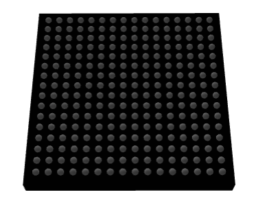
EPM3256AFC256-7 Pin-Out Diagram
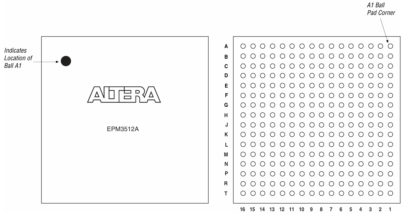
The pin-out diagram of the EPM3256AFC256-7 (similar to the one shown for EPM3512A) illustrates the physical ball grid layout and orientation of the device’s BGA package. On the left, the black dot marks the Ball A1 location, which serves as an orientation reference for proper alignment during PCB placement and soldering. On the right, the grid shows the ball matrix labeled with letters (rows A–T) and numbers (columns 1–16), forming a coordinate system to identify each signal or power ball precisely. This layout ensures accurate mapping between the chip’s internal logic and external pins, allowing to correctly route signals, power, and ground connections on the PCB.
EPM3256AFC256-7 CAD Models
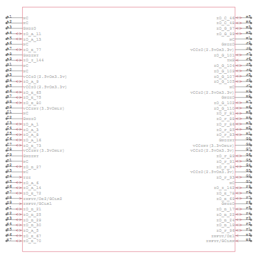
EPM3256AFC256-7 Symbol
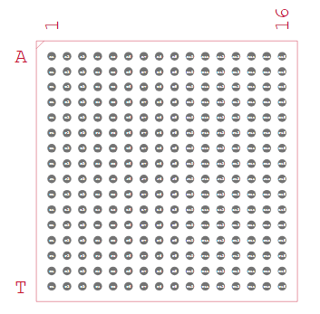
EPM3256AFC256-7 Footprint
EPM3256AFC256-7 3D Model
EPM3256AFC256-7 Features
• Non-Volatile EEPROM-Based Architecture
The device uses EEPROM cells to store configuration data, allowing it to retain its programmed logic even when powered off. Unlike SRAM-based FPGAs, it does not need an external configuration device at startup, which simplifies board design and reduces system cost.
• 256 Macrocells and 16 LABs
It provides 256 programmable macrocells organized into 16 Logic Array Blocks (LABs), giving ample capacity for implementing complex logic functions. Each macrocell supports both combinatorial and registered modes, making it flexible for various logic structures.
• Approx. 5,000 Usable Gates
With around 5,000 gate equivalents, the device can replace multiple TTL or PAL devices in a single chip. This consolidation reduces board space, interconnect complexity, and improves overall system reliability.
• High-Speed Operation (7.5 ns tPD)
The device supports fast propagation delays of approximately 7.5 ns and clock-to-output delays of about 4.8 ns. This performance enables reliable implementation of high-frequency designs up to around 126 MHz depending on the application.
• In-System Programmable via JTAG
EPM3256AFC256-7 supports programming through a standard IEEE 1149.1 JTAG interface, allowing configuration without removing the chip from the PCB. This simplifies development, debugging, and field upgrades.
• MultiVolt I/O Support
Its I/O pins support multiple voltage levels including 2.5 V and 3.3 V operation, while inputs are tolerant up to 5 V. This allows the device to interface with a wide variety of legacy and modern logic families without level shifters.
• Up to 161 User I/O Pins
The chip offers a high number of user-accessible I/O pins, giving flexibility for wide bus interfaces or multiple control signals. The I/O structure supports slew-rate control and open-drain outputs for noise reduction and bus applications.
• Slew-Rate Control & Power Optimization
Each output can be configured for fast or slow slew rate to balance speed with signal integrity. Additionally, macrocells can be individually set to low-power mode on non-critical paths, reducing overall device power consumption.
• Internal Programming Voltage Generation
The device generates its own programming voltages internally, eliminating the need for external high-voltage supplies during programming. This feature simplifies board power design and improves programming convenience.
• Security Bit Protection
A programmable security bit can be set to prevent unauthorized readback of the device’s contents. This feature protects intellectual property and helps maintain the security of proprietary designs.
• TTL/CMOS Compatibility
The CPLD can directly interface with standard TTL and CMOS logic levels. This compatibility makes it easy to integrate into existing systems and replace older programmable logic devices without major redesigns.
• Deterministic Timing Performance
The internal routing structure provides predictable delays, allowing to accurately analyze worst-case timing during development. This makes the device highly suitable for timing-critical control and interface logic.
MAX 3000A Block Diagram
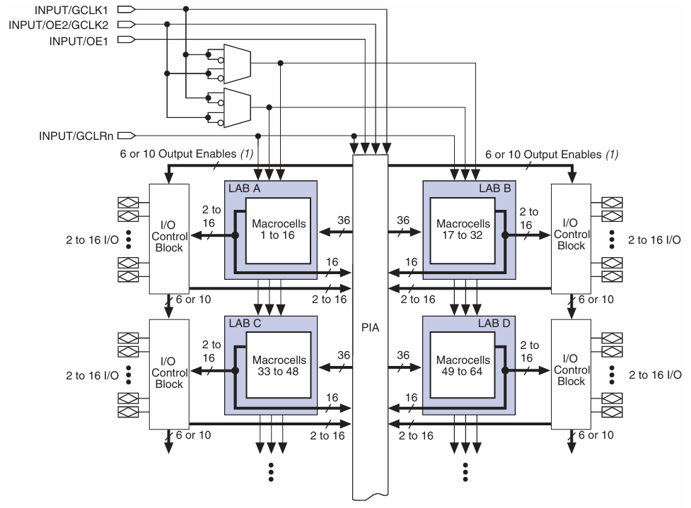
The MAX 3000A block diagram illustrates the internal structure that defines how logic is implemented inside devices like the EPM3256AFC256-7. At the core is the Programmable Interconnect Array (PIA), which links multiple Logic Array Blocks (LABs), each containing several macrocells for building combinational and sequential logic. Surrounding the LABs are I/O control blocks, which handle the interaction between internal logic and external pins, supporting features like output enables and global control signals. This organized architecture allows the device to efficiently implement complex digital functions with predictable timing and flexible routing, making it ideal for control logic, glue logic, and system integration tasks.
ICC vs. Frequency for MAX 3000A Devices
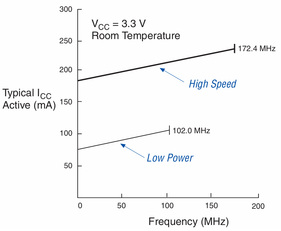
The graph shows how the active supply current of MAX 3000A devices like the EPM3256AFC256-7 varies with operating frequency at 3.3 V and room temperature. Two operating modes are highlighted: Low Power, which reduces current consumption at lower frequencies, and High Speed, which supports higher frequencies but requires more current. As frequency increases, the active current rises, reaching about 172 mA at 172.4 MHz in high-speed mode and around 102 mA at 102 MHz in low-power mode. This relationship is important for power budgeting and thermal design, helping you choose the right balance between performance and energy efficiency for their applications.
EPM3256AFC256-7 Specifications
|
Type |
Parameter |
|
Manufacturer |
Altera/Intel |
|
Series |
MAX® 3000A |
|
Packaging |
Tray |
|
Part Status |
Obsolete |
|
Programmable Type |
In System Programmable |
|
Delay Time tpd(1) Max |
7.5 ns |
|
Voltage Supply – Internal |
3 V ~ 3.6 V |
|
Number of Logic Elements/Blocks |
16 |
|
Number of Macrocells |
256 |
|
Number of Gates |
5000 |
|
Number of I/O |
161 |
|
Operating Temperature |
0 °C ~ 70 °C (TA) |
|
Mounting Type |
Surface Mount |
|
Package / Case |
256-BGA |
|
Supplier Device Package |
256-FBGA (17 × 17) |
|
Base Product Number |
EPM3256 |
EPM3256AFC256-7 Applications
1. Glue Logic and Signal Translation
EPM3256AFC256-7 is widely used as glue logic to connect different digital components within a system. It can perform address decoding, data multiplexing, or protocol bridging between subsystems that operate at different voltage levels or timing domains. By consolidating multiple discrete logic ICs into a single CPLD, it simplifies PCB layouts, reduces part count, and improves system reliability.
2. State Machines and Control Logic
The device is ideal for implementing custom state machines that control sequences, timing, and coordination between system components. Its predictable timing and non-volatile configuration make it well suited for control functions such as initialization routines, reset management, or operational mode control. This allows to offload control logic from microcontrollers or ASICs, improving overall system performance.
3. Bus Interfaces and Peripheral Wrappers
With its large number of I/O pins and flexible logic structure, the CPLD is excellent for creating bus interfaces, peripheral glue, and protocol converters. It can manage data transfer, arbitration, and synchronization between processors, memories, or external devices. This capability is valuable in mixed-technology systems where different buses or signal standards must communicate seamlessly.
4. Industrial and Consumer Electronic Systems
EPM3256AFC256-7 is commonly found in automation controllers, telecom equipment, medical devices, and other embedded platforms requiring moderate logic density. Its reliable non-volatile configuration, low power operation, and in-system programmability make it well suited for long-life, stable applications. Many benefit from its ability to implement custom logic functions without redesigning hardware, enabling flexible system upgrades.
EPM3256AFC256-7 Similar Parts
|
Specification |
EPM3256AFC256-7 |
EPM3256AFI256-10 |
EPM3256AQC208-7N |
EPM3256AQC208-7 |
EPM3256AFC256-10 |
EPM3256AQI-10N |
|
Device Family |
MAX 3000A |
MAX 3000A |
MAX 3000A |
MAX 3000A |
MAX 3000A |
MAX 3000A |
|
Logic Capacity (Macrocells) |
256 |
256 |
256 |
256 |
256 |
256 |
|
Gate Equivalent |
~5,000 |
~5,000 |
~5,000 |
~5,000 |
~5,000 |
~5,000 |
|
Package Type |
FBGA (Fine-Pitch) |
FBGA (Fine-Pitch) |
QFP 208-pin |
QFP 208-pin |
FBGA (Fine-Pitch) |
QFP / Similar |
|
Pin Count |
256 |
256 |
208 |
208 |
256 |
208 |
|
Speed Grade |
-7 |
-10 |
-7 |
-7 |
-10 |
-10 |
|
Supply Voltage (VCC) |
3.0 – 3.6 V |
3.0 – 3.6 V |
3.0 – 3.6 V |
3.0 – 3.6 V |
3.0 – 3.6 V |
3.0 – 3.6 V |
|
I/O Count |
Up to 161 |
Up to 161 |
Slightly fewer (QFP) |
Slightly fewer (QFP) |
Up to 161 |
Slightly fewer |
|
Operating Temperature |
0 °C to +70 °C |
0 °C to +70 °C |
0 °C to +70 °C |
0 °C to +70 °C |
0 °C to +70 °C |
0 °C to +70 °C |
|
Application Focus |
Balanced speed & I/O |
Higher speed variant |
Compact board layout |
Non-RoHS variant |
Faster in same pkg |
Alt. package for legacy systems |
EPM3256AFC256-7 Programming Steps
Before you can use the EPM3256AFC256-7, you need to load your custom logic design into the device through its JTAG interface. This process ensures the CPLD is correctly configured and ready to perform its intended functions in your system.
1. Design and Compile Your Project
You begin by creating your design using a development tool such as Intel Quartus. This involves writing HDL code or drawing schematics, assigning I/O pins, and setting timing constraints. Once complete, you compile the project to generate a programming file (usually a .pof or .jam) that contains all the configuration data needed for the CPLD.
2. Connect the JTAG Programmer and Hardware
Next, you power the board with the proper voltage levels and connect a JTAG cable (e.g., USB-Blaster) to the device’s JTAG header. Make sure the TCK, TMS, TDI, and TDO pins are correctly wired to avoid communication errors. A stable power supply and correct orientation of the cable are needed to ensure smooth programming.
3. Select the Device and Load the Programming File
In your programming software, you detect the JTAG chain and verify that the EPM3256AFC256-7 appears correctly. You then load the compiled programming file and select the proper operations such as Program, Configure, and Verify. This step ensures the tool knows exactly what file to load and how to program the target device.
4. Erase, Program, and Verify the Device
The software first erases any existing configuration inside the CPLD’s non-volatile memory. It then writes the new logic configuration into the device and performs a verification step to confirm successful programming. This ensures the internal EEPROM now contains your exact design and will retain it even when power is removed.
5. Perform Post-Programming Checks
After programming, you test the device by applying input signals and verifying that outputs behave as expected. You should also check for pin conflicts or incorrect routing that might affect functionality. If any issues arise, you can easily reprogram the CPLD through JTAG without removing it from the PCB.
EPM3256AFC256-7 Advantages and Disadvantages
Advantages
• Starts operating instantly at power-up without external configuration.
• Offers stable and predictable timing for reliable designs.
• Consumes less static power than larger FPGAs.
• Lowers overall system cost and simplifies board design.
• Easy to reprogram and debug directly in the system.
Disadvantages
• Limited logic capacity for large or complex designs.
• Lower maximum performance compared to modern devices.
• Risk of obsolescence and limited long-term availability.
• Lacks advanced features found in newer programmable logic.
• Less scalable for future design expansions.
EPM3256AFC256-7 Packaging Dimensions
|
Type |
Parameter |
|
Package Type |
256-FBGA (Fine-Pitch Ball Grid Array) |
|
Package Size (D × E) |
17.00 mm × 17.00 mm (BSC) |
|
Maximum Package Height (A) |
2.60 mm |
|
Standoff / Ball Height (A1) |
0.35 mm (minimum) |
|
Ball Grid Pitch (e) |
1.00 mm (nominal) |
|
Ball Diameter (b) |
0.50 mm – 0.60 mm (typical) |
|
Coplanarity (Maximum) |
0.20 mm |
|
Mounting Type |
Surface Mount |
|
Supplier Device Package |
256-FBGA (17 × 17) |
EPM3256AFC256-7 Manufacturer
The EPM3256AFC256-7 is manufactured by Altera, a pioneer in programmable logic device technology. Altera became widely known for its CPLDs and FPGAs, which set industry standards for performance, flexibility, and integration. In 2015, Intel acquired Altera, and the device is now part of Intel’s Programmable Solutions Group, ensuring continued support and integration within Intel’s product ecosystem.
Conclusion
The EPM3256AFC256-7 stands out for its non-volatile EEPROM-based architecture, fast timing performance, and flexible I/O capabilities, making it a dependable choice for control logic, glue logic, and bus interfacing in embedded and industrial systems. Its deterministic behavior, in-system programmability, and multi-voltage support simplify design integration and maintenance. Although it offers moderate logic capacity and faces obsolescence compared to modern alternatives, its reliability and ease of use have kept it relevant in many stable, long-lifecycle applications.
Datasheet PDF
EPM3256AFC256-7 Datasheets:
About us
ALLELCO LIMITED
Read more
Quick inquiry
Please send an inquiry, we will respond immediately.
Frequently Asked Questions [FAQ]
1. Can the EPM3256AFC256-7 replace older TTL or PAL logic devices in my design?
Yes. With approximately 5,000 usable gates and TTL/CMOS compatibility, the EPM3256AFC256-7 can replace multiple discrete TTL or PAL ICs, reducing board space and simplifying routing while improving reliability.
2. Does the EPM3256AFC256-7 require external configuration memory?
No. It uses EEPROM technology, so the configuration is stored internally and automatically loads at power-up. This removes the need for any external configuration device, simplifying your board design.
3. How does the EPM3256AFC256-7 handle mixed-voltage environments?
Its I/O pins support 2.5 V and 3.3 V operation, with inputs tolerant up to 5 V. This allows you to connect it directly to both legacy and modern logic levels without needing external level shifters.
4. What programmer is recommended for the EPM3256AFC256-7?
The device supports in-system programming through the standard IEEE 1149.1 JTAG interface. Intel’s USB-Blaster or equivalent JTAG programmers are typically used.
5. How does the EPM3256AFC256-7 compare to modern FPGAs?
Unlike modern FPGAs that rely on external memory, the EPM3256AFC256-7 stores configuration internally. It is simpler, consumes less power, and boots instantly, though it has lower capacity and speed compared to today’s devices.
XC2C256-7TQ144C CPLD: Pinout, Features, Programming and Datasheet Guide
on October 3th
EP1C4F400C8 FPGA: Features, Specifications, Programming and Alternatives
on October 2th
Popular Posts
-

Complex Instruction Set Computers: How They Changed Computing?
on April 18th 147749
-

USB-C Pinout and Features
on April 18th 111916
-

Using Xilinx Unified Simulation Primitives: A Comprehensive Guide to FPGA Design and Simulation
on April 18th 111349
-

Power Supply Voltages in Electronics: Meaning of VCC, VDD, VEE, VSS, and GND
on April 18th 83714
-

RJ45 Connector Guide: Pinout, Wiring, Cable Types, and Uses
on January 1th 79502
-

The Ultimate Guide to Wire Color Codes in Modern Electrical Systems
The way our electrical systems use colors isn’t just for looks. Each wire color now indicates a specific function, making it easier to identify and handle electrical components correctly during ins...on January 1th 66872
-

Quality (Q) Factor: Equations and Applications
The quality factor, or 'Q', is important when checking how well inductors and resonators work in electronic systems that use radio frequencies (RF). 'Q' measures how well a circuit minimizes energy...on January 1th 63005
-

Purge Valve Guide: Function, Symptoms, Testing, and Replacement for Optimal Engine Performance
The purge valve is a key part of a car’s system that helps keep the air clean by managing fuel vapors before they can escape into the atmosphere. This not only helps the environment by reducing pol...on January 1th 62949
-

Achieving Peak Performance with the Maximum Power Transfer Theorem
The Maximum Power Transfer Theorem explains how energy from a source, such as a battery or generator, flows to a connected load. It shows the exact condition where the load receives the most power....on January 1th 54077
-

A23 Battery Specifications and Compatibility
The A23 battery is a small, cylinder-shaped battery with high voltage. Also called 23A, 23AE, or MN21, it runs at 12 volts and much higher than AA or AAA batteries. Its special design make...on January 1th 52091
HOT Part Number
-

BD9B100MUV-E2
Rohm Semiconductor
IC REG BUCK ADJ 1A 16VQFN
UPD70F3539AF5A9-PN7-Q-A
Renesas Electronics America Inc
IC MICROCONTROLLER
18081A621JAT2A
KYOCERA AVX
CAP CER 620PF 100V NP0 1808
FDN340P
onsemi
MOSFET P-CH 20V 2A SUPERSOT3
70231-101
Amphenol ICC (FCI)
CONN RCPT BLADE PWR 8POS EDGE MT
MPSW42RLRAG
onsemi
TRANS NPN 300V 0.5A TO92
MC7824BT
onsemi
IC REG LINEAR 24V 1A TO220AB
AD8009ARZ-REEL
Analog Devices Inc.
IC OPAMP CFA 1 CIRCUIT 8SOIC
LT1815CS5#TRPBF
Analog Devices Inc.
IC OPAMP VFB 1 CIRCUIT TSOT23-5
DG411DYZ
Renesas Electronics America Inc
IC SWITCH SPST-NCX4 35OHM 16SOIC
VFT2060C-M3/4W
Vishay General Semiconductor - Diodes Division
DIODE SCHOTTKY 20A 60V ITO-220AB
TSX562AIYST
STMicroelectronics
IC CMOS 2 CIRCUIT 8MINISO
MR256D08BMA45
Everspin Technologies Inc.
IC RAM 256KBIT PARALLEL 48FBGA
VSC3312YYP-01
Microchip Technology
IC SWITCH 16X16 6.5GBPS 196FCBGA
XC68HC908GP20CFB
Motorola
TSG 8BIT20K FLASH
CSR8811A08-ICXR-R
Qualcomm
IC RF TXRX+MCU BLUETOOTH
MPSW05
onsemi
TRANS NPN 60V 0.5A TO92
1N4055R
Solid State Inc.
DIODE GEN PURP REV 900V 275A DO9 -

ASX342ATSC00XPED0-DP
onsemi
IMAGE SENSOR VGA 1/4 CIS SOC
0433.125NR
Littelfuse Inc.
FUSE BOARD MNT 125MA 125VAC/VDC
1SMA5941BT3G
onsemi
DIODE ZENER 47V 1.5W SMA
DCP010512BP-U/700
Texas Instruments
DC DC CONVERTER 12V 1W
1-1734344-1
TE Connectivity AMP Connectors
CONN D-SUB HD RCPT 15P R/A SLDR
KSD1621STF
onsemi
TRANS NPN 25V 2A SOT89-3
BQ24161RGET
Texas Instruments
IC BATT CHG LI-ION 1CELL 24VQFN
BTA26-600BW
STMicroelectronics
TRIAC ALTERNISTOR 600V 25A TOP3
NCP1239DD65R2G
onsemi
IC OFFLINE SWITCH FLYBACK 7SOIC
TMS320TCI6482BZTZA
Texas Instruments
TMS320 - DIGITAL SIGNAL PROCESSO
BQ20Z90DBTR-V150
Texas Instruments
IC GAS GAUGE LI-ION 30TSSOP
PCMB104T-1R0MT
Susumu
FIXED IND 1UH 18A 3.3 MOHM SMD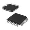
CY29942AXCT
Infineon Technologies
IC CLK BUFFER 1:18 200MHZ 32TQFP
CC0402KRX7R9BB561
YAGEO
CAP CER 560PF 50V X7R 0402
STPS20M60SG-TR
STMicroelectronics
DIODE SCHOTTKY 60V 20A D2PAK
AT25010N-10SC-2.7
Microchip Technology
IC EEPROM 1KBIT SPI 3MHZ 8SOIC
04023A1R0CAT4A
KYOCERA AVX
CAP CER 1PF 25V C0G/NP0 0402
ISL6327IRZ
Intersil
SWITCHING CONTROLLER, VOLTAGE-MO -

LQW18AN75NG0ZD
Murata Electronics
FIXED IND
DFA100BA160
SanRex Corporation
DIODE MODULE 1600V 100A
BAR46AFILM
STMicroelectronics
DIODE ARRAY SCHOTTKY 100V SOT23
MAX825SEUK
Analog Devices Inc./Maxim Integrated
IC SUPERVISOR MPU
MMST2222A-7-F
Diodes Incorporated
TRANS NPN 40V 0.6A SOT323
FODM8801AR2
onsemi
OPTOISO 3.75KV TRANS 4-MINI-FLAT
FJV1845FMTF
Fairchild Semiconductor
SMALL SIGNAL BIPOLAR TRANSISTOR,
EVK105RH5R1JW-F
Taiyo Yuden
CAP CER 5.1PF 16V R2H 0402
6651170-3
TE Connectivity AMP Connectors
CONN EDGE DUAL FMALE 4POS 0.508
KSZ8893FQLI-FX
Microchip Technology
IC SWITCH ETH 3PORT 128QFP
170M6340
Eaton - Bussmann Electrical Division
FUSE SQUARE 400A 1.3KVAC RECT
BCM20741A2KFB1G
Broadcom Limited
SINGLE-CHIP BLUETOOTH
MAX3443EASA+
Analog Devices Inc./Maxim Integrated
IC TRANSCEIVER HALF 1/1 8SOIC
GRM0335C1H9R3DA01D
Murata Electronics
CAP CER 9.3PF 50V C0G/NP0 0201
TNY175PN
Power Integrations
11.5 W (85-265 VAC) 15 W (230 VA
742700726
Würth Elektronik
FERRITE CORE 278 OHM SOLID 4MM
DM74S20N
onsemi
IC GATE NAND 2CH 4-INP 14DIP
P4SMA56CA-E3/61
Vishay General Semiconductor - Diodes Division
TVS DIODE 47.8VWM 77VC DO214AC