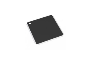
LC5768MC-75F256C CPLD: Features, Specs, Advantages and Applications
This guide explains the LC5768MC-75F256C, a small but powerful chip made by Lattice Semiconductor. It shows what the chip does, how it works, how to program it, and where it can be used. If you're looking for a chip that handles logic tasks, uses low power, and works in many devices, this guide will help you understand why the LC5768MC-75F256C is a good option.Catalog
What is the LC5768MC-75F256C?
The LC5768MC-75F256C is a high-performance Complex Programmable Logic Device (CPLD), part of the ispXPLD 5000MC family. This device is designed around a 1.8V core architecture and provides robust logic density, integrating 768 macrocells. As a member of the 5000MC series, it represents Lattice’s advanced CPLD solutions that offer reliable timing control, efficient logic implementation, and low power operation, all optimized for embedded and high-speed digital systems. The ispXPLD 5000MC family enhances the capabilities of traditional CPLDs by introducing Multi-Function Blocks (MFBs) and flexible I/O support, making the LC5768MC-75F256C a solid choice for scalable logic integration. With its proven reliability and architecture tailored for deterministic performance, this device serves as a dependable building block in digital design.
Looking for LC5768MC-75F256C? Contact us to check current stock, lead time, and pricing.
LC5768MC-75F256C Features
• 768 Macrocells (MFB-Based Architecture)
The device integrates 768 macrocells organized in advanced Multi-Function Blocks (MFBs), supporting high-density logic with embedded arithmetic and memory capabilities. These MFBs allow flexible configuration for logic, dual-port SRAM, FIFO, and CAM functions.
• 1.8V Core Voltage (MC Variant)
This MC-series variant operates with a 1.8V core, offering lower power consumption for portable and high-efficiency designs. Despite the low voltage, it maintains robust performance and logic density.
• 7.5 ns Propagation Delay (Speed Grade -75)
It achieves a maximum pin-to-pin propagation delay of just 7.5 nanoseconds, making it suitable for moderate- to high-speed digital applications. The -75 speed grade balances power and speed in embedded systems.
• 193 Programmable I/O Pins
The chip offers 193 I/O pins that support multiple voltage standards and protocols. These pins are fully programmable and allow flexible interfacing with other logic or analog devices.
• SuperWIDE Logic Support (Up to 136 Inputs per Block)
Each MFB supports very wide logic functions with up to 136 input signals, enabling complex combinational logic in fewer logic levels. This reduces propagation delay and simplifies logic synthesis.
• Embedded Dual-Port SRAM, FIFO, and Ternary CAM Support
MFBs are configurable to act as SRAM (single/dual port), FIFOs, or ternary Content Addressable Memory. This flexibility enables memory-rich logic design in a compact CPLD.
• On-Chip PLL (sysCLOCK™)
The built-in PLL supports clock multiplication/division from 1× to 32×, phase shifting, and external feedback. It helps manage timing and skew across high-speed synchronous systems.
• Wide I/O Standard Support (sysIO™)
The I/O blocks support a broad range of signaling standards including LVCMOS, LVTTL, SSTL, HSTL, GTL+, LVDS, and LVPECL. This enables mixed-voltage and differential signaling on a single device.
• In-System Programmability (ispXP™)
The device supports in-system programming through IEEE 1532 or sysCONFIG interface. It can be reprogrammed on the board without removing it, enabling design updates and field reconfiguration.
• Boundary Scan Test (IEEE 1149.1 Compliant)
Full JTAG boundary scan support allows robust board-level testing and debugging. This ensures compliance with modern test requirements and simplifies validation in production.
• 5V Tolerant I/O
Despite a 1.8V core, the I/O banks are tolerant of 5V signals, supporting legacy voltage interfaces. This improves compatibility with older systems and mixed-voltage environments.
ispXPLD 5000MX/5000MC Block Diagram
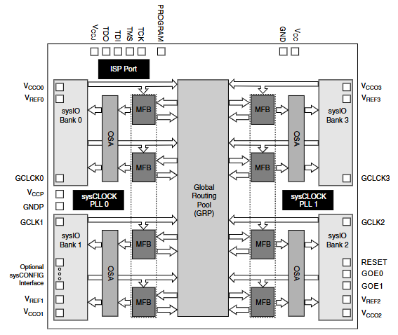
The block diagram of the LC5768MC-75F256C in the ispXPLD 5000MX/5000MC family highlights how the chip is structured to handle programmable logic tasks. At the center is the Global Routing Pool (GRP), which acts as the main connection hub, linking various logic and functional blocks so signals can move efficiently throughout the device. On either side of the GRP are two Phase-Locked Loops (PLL0 and PLL1), part of the sysCLOCK system. These generate precise and adjustable clock signals that help maintain timing accuracy for high-speed operations across the chip.
Around the GRP and PLLs are four sysIO Banks. Each bank contains Configurable System Arrays (CSAs) and Multi-Function Blocks (MFBs). The CSAs handle basic logic processing, while the MFBs support more advanced features like math operations and memory functions. This arrangement gives the device strong I/O flexibility and makes it easier to scale for different applications. Power and clock connections are also clearly shown in the diagram. Multiple VCC, VREF, and GND pins are distributed to maintain stable power across the chip. Global clock inputs (GCLK0 to GCLK3) allow external clocks to feed into the system and work with the GRP and PLLs.
Multi-Function Block (MFB) Diagram
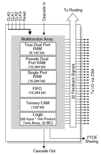
The Multi-Function Block (MFB) in the LC5768MC-75F256C ispXPLD 5000MX/5000MC combines both memory and logic functions to support flexible design needs. It supports several memory types, including True Dual Port RAM (8,192 bits), Pseudo Dual Port RAM, FIFO, and Single Port RAM (each up to 16,384 bits), plus Ternary CAM (128×48). These memory options make the MFB useful for data buffering, temporary storage, and fast data lookup.
The MFB also has strong logic capabilities. It includes a 68-input by 164-product term array and 32 Macrocells, allowing it to perform complex logic operations. It uses multiple clock inputs (CLK0 to CLK3) and a reset signal to control timing and operations. To expand functionality, Cascade In/Out ports allow MFBs to be connected together across blocks. The QSA (Quad System Array) interface connects the MFB to I/O banks for fast communication with external systems. In short, the MFB is a powerful, flexible unit that handles both memory and logic tasks, helping the device perform well in embedded and high-speed applications.
LC5768MC-75F256C Specifications
|
Type |
Parameter |
|
Manufacturer |
Lattice Semiconductor Corporation |
|
Series |
ispXPLD® 5000 |
|
Packaging |
Bulk |
|
Part Status |
Active |
|
Programmable Type |
In System Programmable |
|
Delay Time tpd(1) Max |
7.5 ns |
|
Voltage Supply - Internal |
1.65V ~ 1.95V |
|
Number of Logic Elements/Blocks |
24 |
|
Number of Macrocells |
768 |
|
Number of I/O |
193 |
|
Operating Temperature |
0°C ~ 90°C (TJ) |
|
Mounting Type |
Surface Mount |
|
Package / Case |
256-BGA |
|
Supplier Device Package |
256-FPBGA (17x17) |
LC5768MC-75F256C Applications
1. Telecommunications and Networking
The LC5768MC-75F256C is ideal for use in base stations, telecom switches, and optical network units, where high-speed and deterministic logic are needed. Its embedded memory and multi-voltage I/O support enable protocol processing, data framing, and low-latency control tasks.
2. Data Communication and Storage
This CPLD is well-suited for routers, RAID controllers, and disk-array systems that require efficient data handling and fast signal processing. Its dual-port SRAM and FIFO support provide the buffering and flow control needed in high-throughput environments.
3. Protocol Processors and Bus Interfaces
With predictable timing and high-density logic resources, the LC5768MC excels in implementing bus bridges, backplane interfaces, and protocol decoders. It enables quick logic responses and supports seamless integration with multiple signaling standards.
4. Industrial and IoT Control Systems
In industrial automation, the device is used for monitoring, machine control, and logic sequencing. Its instant-on capability, low power draw, and robust I/O features make it suitable for IoT nodes and embedded controllers.
5. Consumer and Medical Electronics
The compact footprint and rich logic-mixed-memory capabilities make this CPLD valuable in portable medical instruments and consumer electronics. It handles system control, interface management, and power sequencing in size-constrained and energy-sensitive designs.
LC5768MC-75F256C Similar Parts
|
Feature |
LC5768MC-75F256C |
LC5768MV-75F484C |
LC5768MV-75FN256C |
LC5768MV-5F484C |
|
Family |
ispXPLD 5000MC |
ispXPLD 5000MV |
ispXPLD 5000MV |
ispXPLD 5000MV |
|
Core Voltage |
1.8 V |
3.3 V |
3.3 V |
3.3 V |
|
Macrocells |
768 |
768 |
768 |
768 |
|
Max Frequency |
~150 MHz |
~150 MHz |
~150 MHz |
~200–250 MHz |
|
Propagation Delay (tpd) |
7.5 ns |
7.5 ns |
7.5 ns |
5 ns |
|
Package Type |
256-ball BGA |
484-ball BGA |
256-ball BGA |
484-ball BGA |
|
Package Code |
F256C |
F484C |
FN256C |
F484C |
|
I/O Count |
193 |
317 |
193 |
317 |
|
In-System Programmable |
Yes |
Yes |
Yes |
Yes |
|
Embedded Memory Support |
Yes (SRAM/FIFO/CAM) |
Yes |
Yes |
Yes |
|
JTAG (IEEE 1149.1) |
Supported |
Supported |
Supported |
Supported |
|
Instant-On |
Yes |
Yes |
Yes |
Yes |
|
Application |
Low-power, dense logic |
High I/O, general CPLD |
Compact 3.3 V logic |
High-speed 3.3 V logic |
LC5768MC-75F256C Programming Steps
1. Prepare Your Board and Tools
Connect the LC5768MC-75F256C to your PC using a compatible programming cable such as the Lattice HW-USBN-2B. Make sure JTAG lines are properly routed and termination resistors (e.g., 4.7kΩ on TCK) are in place to ensure stable communication.
2. Generate the Programming File
Use Lattice Diamond or ispVM software to compile your design and export a JEDEC (.jed) programming file. This file contains the complete bitstream that will be written into the CPLD’s configuration memory.
3. Launch the Programming Software
Open the Diamond Programmer or ispVM System tool on your PC and verify that your programmer is properly detected. Select the LC5768MC-75F256C device from the list to begin setup.
4. Execute In-System Programming (ISP)
Use the JTAG (IEEE 1532) interface to load the JEDEC file directly into the device while it remains mounted on the board. The bitstream is stored in internal non-volatile memory, enabling instant-on configuration at startup.
5. Verify and Secure Configuration
After programming, perform a read-back operation to confirm the configuration was successful. If required, activate the security fuse to lock the device and prevent unauthorized reprogramming or reverse engineering.
6. Configure and Reset the Device
Once programming is complete, the device may automatically restart, or you can toggle its PROGRAM or INIT pins to force a reload. The CPLD will then operate based on the newly applied configuration with deterministic startup timing.
7. Optional: Field Reprogramming or Updates
You can reprogram the LC5768MC-75F256C in the field using the same JTAG interface for updates or corrections. Additionally, its sysCONFIG™ interface allows partial reconfiguration without full power cycling in advanced applications.
LC5768MC-75F256C Advantages
• Lower Power Operation for Portable and Embedded Systems
Compared to many traditional CPLDs with higher core voltages, the LC5768MC-75F256C’s low-power 1.8V core helps reduce overall system power consumption. This makes it attractive for battery-operated or heat-sensitive applications where thermal budget and energy efficiency matter.
• Instant-On Capability
Unlike many FPGAs or larger programmable devices that require external configuration at every startup, this CPLD offers instant-on behavior, allowing to avoid delays or the need for external flash memory. This leads to faster time-to-operation and greater reliability.
• More Predictable Timing vs. FPGAs
The deterministic timing behavior of this CPLD, especially under heavy logic or I/O loads, gives better control compared to the often-variable timing of larger FPGAs. This makes it more suitable for time-critical applications like digital control loops, communication interfaces, and synchronized logic systems.
• Efficient Learning Curve and Design Tool Ecosystem
For transitioning from 22V10s, older PAL/GALs, or simple PLDs, this device offers a gentle learning curve via Lattice’s intuitive design tools like Diamond and ispVM. Many benefit from faster prototyping and fewer integration headaches.
LC5768MC-75F256C Packaging Dimensions
• Package Type: Fine-pitch Ball Grid Array
• Pin Count: 256 balls
• Package Size: 17 mm × 17 mm
• Package Height: Approximately 1.2 mm
• Ball Pitch: Standard fine-pitch usually 0.8 mm
LC5768MC-75F256C Manufacturer
The LC5768MC-75F256C is manufactured by Lattice Semiconductor Corporation, a U.S.-based company recognized for its expertise in low-power, small-footprint programmable logic devices. Founded in 1983 and headquartered in Hillsboro, Oregon, Lattice focuses on delivering FPGAs, CPLDs, and related development tools tailored for applications in communications, computing, industrial, automotive, and consumer markets. The company is known for long product lifecycles, broad design tool support, and reliable in-system programmability across its device families. As the original developer and supplier of the ispXPLD® 5000MC family, Lattice ensures robust technical documentation, software support, and availability through authorized distributors and long-term lifecycle partners.
Conclusion
The LC5768MC-75F256C is a smart and reliable CPLD that offers strong logic and memory functions in one compact chip. It uses little power, starts up instantly, and works with many different signal types. With 768 macrocells, built-in memory, fast clocking, and flexible input/output options, it fits well in products like telecom devices, industrial machines, storage systems, and consumer electronics. Its easy programming, strong performance, and support for updates make it a helpful solution for both new designs and upgrades.
About us
ALLELCO LIMITED
Read more
Quick inquiry
Please send an inquiry, we will respond immediately.
Frequently Asked Questions [FAQ]
1. Can I use the LC5768MC-75F256C in battery-powered or energy-sensitive devices?
Yes, the 1.8V core voltage and low-power design of the LC5768MC-75F256C make it highly suitable for portable, battery-operated, and thermally constrained environments, such as IoT nodes or medical devices.
2. Is the LC5768MC-75F256C compatible with legacy 5V systems?
Yes. Even with its low core voltage, the LC5768MC-75F256C features 5V-tolerant I/O banks, ensuring compatibility with legacy interfaces and mixed-voltage systems without requiring additional level-shifting components.
3. What kind of development tools are supported for LC5768MC-75F256C programming?
The LC5768MC-75F256C is supported by Lattice Diamond, ispVM System, and the Diamond Programmer. These tools provide complete support for design, simulation, programming, and debugging suitable for both entry-level and advanced users.
4. Does the LC5768MC-75F256C require external memory to operate?
No external memory is required for configuration. The LC5768MC-75F256C has non-volatile memory and supports instant-on capability, allowing it to begin operation immediately after power-up without needing external flash or EEPROM.
5. Is the LC5768MC-75F256C suitable for harsh industrial environments?
Yes, with robust logic performance, wide voltage tolerance, and reliable startup behavior, the LC5768MC-75F256C performs well in industrial control systems and factory automation where stable operation is needed.
EPF8820ARC208-4 FPGA Guide: Features, Architecture, Applications, and Programming
on July 11th
EPF6016ATC144-2N FPGA: Features, Programming, Applications, and Alternatives
on July 10th
Popular Posts
-

Complex Instruction Set Computers: How They Changed Computing?
on April 18th 147764
-

USB-C Pinout and Features
on April 18th 111984
-

Using Xilinx Unified Simulation Primitives: A Comprehensive Guide to FPGA Design and Simulation
on April 18th 111351
-

Power Supply Voltages in Electronics: Meaning of VCC, VDD, VEE, VSS, and GND
on April 18th 83743
-

RJ45 Connector Guide: Pinout, Wiring, Cable Types, and Uses
on January 1th 79538
-

The Ultimate Guide to Wire Color Codes in Modern Electrical Systems
The way our electrical systems use colors isn’t just for looks. Each wire color now indicates a specific function, making it easier to identify and handle electrical components correctly during ins...on January 1th 66948
-

Purge Valve Guide: Function, Symptoms, Testing, and Replacement for Optimal Engine Performance
The purge valve is a key part of a car’s system that helps keep the air clean by managing fuel vapors before they can escape into the atmosphere. This not only helps the environment by reducing pol...on January 1th 63087
-

Quality (Q) Factor: Equations and Applications
The quality factor, or 'Q', is important when checking how well inductors and resonators work in electronic systems that use radio frequencies (RF). 'Q' measures how well a circuit minimizes energy...on January 1th 63028
-

Achieving Peak Performance with the Maximum Power Transfer Theorem
The Maximum Power Transfer Theorem explains how energy from a source, such as a battery or generator, flows to a connected load. It shows the exact condition where the load receives the most power....on January 1th 54092
-

A23 Battery Specifications and Compatibility
The A23 battery is a small, cylinder-shaped battery with high voltage. Also called 23A, 23AE, or MN21, it runs at 12 volts and much higher than AA or AAA batteries. Its special design make...on January 1th 52171
HOT Part Number
-

50YXJ330M10X20
Rubycon
CAP ALUM 330UF 20% 50V RADIAL
CY7B993V-2AXI
Infineon Technologies
IC CLK BUFF 100TQFP
CPC1972GS
IXYS Integrated Circuits Division
SSR RELAY SPST-NO 250MA 0-800V
CPC1593GSTR
IXYS Integrated Circuits Division
SSR RELAY SPST-NO 120MA 0-600V
TDA7350A
STMicroelectronics
IC AMP AB MONO/STER 11MULTIWATT
FDC604P
onsemi
MOSFET P-CH 20V 5.5A SUPERSOT6
170M2713
Eaton - Bussmann Electrical Division
FUSE SQUARE 80A 690VAC RECT
P6KE130CA
SMC Diode Solutions
TVS DIODE 111VWM 179VC DO15
ATF22LV10C-10SU
Microchip Technology
IC PLD 10MC 10NS 24SOIC
UMK107CG181JZ-T
Taiyo Yuden
CAP CER 180PF 50V C0G/NP0 0603
CL03C020BA3GNNH
Samsung Electro-Mechanics
CAP CER 2PF 25V NP0 0201
MCP1700T-2502E/TT
Microchip Technology
IC REG LINEAR 2.5V 250MA SOT23-3
MC14066BDTR2
onsemi
IC BILATERAL SW 1 X 1:1 14TSSOP
CD74HCT14M
Texas Instruments
IC INV SCHMITT 6CH 1-IN 14SOIC
PS2565L1-1-V-A
Renesas Electronics America Inc
OPTOISOLATOR 5KV TRANS 4DIP
DG302AAK/883
Vishay Siliconix
IC SW DPST-NOX2 50OHM 14CERDIP
IRF7353D2TRPBF
Infineon Technologies
MOSFET N-CH 30V 6.5A 8SO
TPS71750DSET
Texas Instruments
IC REG LINEAR 5V 150MA 6WSON -
BZT52C3V3T-7
Diodes Incorporated
DIODE ZENER 3.3V 300MW SOD523
TLV5580CDW
Texas Instruments
IC ADC 8BIT PIPELINED 28SOIC
P0720SC
Littelfuse Inc.
THYRISTOR 65V 400A DO214AA
D2SW-01L1H
Omron Electronics Inc-EMC Div
SWITCH SNAP ACT SPDT 100MA 125V
VI-26N-IW
Vicor Corporation
DC DC CONVERTER 18.5V 100W
IKW15N120H3
Infineon Technologies
IKW15N120 - DISCRETE IGBT WITH A
SNJ54LS540J
Texas Instruments
54LS540 OCTAL BUFFERS AND LINE D
74LVC8T245PW-Q100J
Nexperia USA Inc.
IC TRANSLATION TXRX 5.5V 24TSSOP
GRM188R61E475KE11J
Murata Electronics
CAP CER 4.7UF 25V X5R 0603
LP3999ITL-3.3
Texas Instruments
IC REG LINEAR FIXED POS LDO REG
CY74FCT16374TPVC
Texas Instruments
IC FF D-TYPE DUAL 8BIT 48SSOP
SMA6J6.0CA
Littelfuse Inc.
TVS DIODE 6VWM 10.3VC DO214AC TR
GRM1555C2A6R6CA01J
Murata Electronics
CAP CER 6.6PF 100V C0G/NP0 0402
EMZR250ARA821MJA0G
United Chemi-Con
CAP ALUM 820UF 20% 25V SMD
NXH80T120L2Q0S2TG
onsemi
MODULE PIM 1200V 80A
SY58018UMG
Microchip Technology
IC MULTIPLEXER 1 X 2:1 16MLF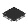
R5F21356MNFP#X4
Renesas Electronics America Inc
IC MCU 16BIT 32KB FLASH 52LQFP
LMH6503MTX
Texas Instruments
IC OPAMP VGA 135MHZ 14TSSOP -

CD4029BCN
onsemi
IC BINARY COUNTER 4-BIT 16DIP
AD8675ARZ-REEL7
Analog Devices Inc.
IC OPAMP GP 1 CIRCUIT 8SOIC
DS1087LU-255+T
Analog Devices Inc./Maxim Integrated
IC CLOCK GENERATOR 8UMAX
IRG7S313UTRLPBF
Infineon Technologies
IGBT PDP 330V 40A D2PAK
LQP03HQ13NH02D
Murata Electronics
FIXED IND 13NH 300MA 500MOHM SMD
STSJ60NH3LL
STMicroelectronics
MOSFET N-CH 30V 60A 8SOIC
10CL025YU256I7G
Intel
IC FPGA 150 I/O 256UBGA
BCM89832A0BWMLG
Broadcom Limited
100BASE-T1 PHY
AD9220ARSZ-REEL
Analog Devices Inc.
IC ADC 12BIT PIPELINED 28SSOP
LT3507AEFE#PBF
Analog Devices Inc.
IC REG QUAD BUCK/LINEAR 38TSSOP
TC4468CPD
Microchip Technology
IC GATE DRVR LOW-SIDE 14DIP
UA78M05QDCYRQ1
Texas Instruments
IC REG LINEAR 5V 500MA SOT223-4
LMS3655NQRNLTQ1
Texas Instruments
IC REG BUCK 3.3V 5.5A 22VQFN
MCL2012H100MT
Shenzhen Sunlord Electronics Co., Ltd.
FIXED IND 10UH 100MA 500MOHM SMD
CGA9N3X7S2A106K230KB
TDK Corporation
CAP CER 10UF 100V X7S 2220
VE-2W4-IV
Vicor Corporation
DC DC CONVERTER 48V 150W
NTMD2C02R2G
onsemi
MOSFET N/P-CH 20V 8SOIC
MAX2654EXT-T
Analog Devices Inc./Maxim Integrated
IC AMP GPS 1.4GHZ-1.7GHZ SC70-6