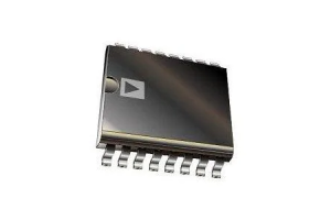
XC2V500-5FGG456C Programmable Logic Device Specs and Uses
You get a clear look at how the XC2V500-5FGG456C fits into real hardware designs and why it has been used across many systems. You see how its logic resources, memory, and I/O structure work together to handle control and data tasks on one chip. The layout, package style, and operating range help you understand where it works best. By walking through features, architecture, and applications, you can quickly judge whether this FPGA matches the performance, flexibility, and layout needs of your next design.Catalog
XC2V500-5FGG456C Overview
The XC2V500-5FGG456C is a programmable logic device designed to support complex digital control and data handling tasks within embedded systems. It allows flexible hardware configuration, enabling multiple logic functions to be implemented on a single chip. The device offers a balance of logic capacity, operating speed, and input output availability, supporting compact board layouts. Its structure accommodates parallel processing and reliable signal coordination across connected components. This part is commonly applied in communication equipment, industrial control platforms, and embedded processing systems where adaptability and stable operation are required. Looking for XC2V500-5FGG456C? Contact us to check current stock, lead time, and pricing.
I/O Banks of XC2V500-5FGG456C
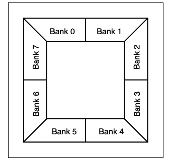
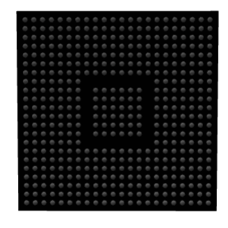
Arranged as a continuous ring around the central logic area, the structure divides the device perimeter into eight distinct I/O banks labeled Bank 0 through Bank 7. Each bank groups a set of pins that share common electrical settings and reference voltages, enabling multiple I/O standards within the same device. The top view reflects the physical placement used in wire bond packages, with banks distributed along all sides to support balanced routing and consistent power distribution across the FPGA.
XC2V500-5FGG456C CAD Model
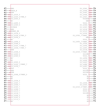
XC2V500-5FGG456C Symbol
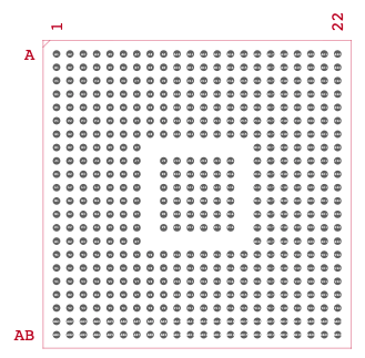
XC2V500-5FGG456C Footprint
XC2V500-5FGG456C 3D Model
Features of XC2V500-5FGG456C
Configurable Logic Capacity
The device includes 768 configurable logic blocks that allow flexible implementation of custom digital functions. These blocks can be arranged to support control tasks, data handling, and signal coordination within a single programmable structure. This flexibility allows multiple logic roles to be combined without adding separate components.
System Gate Density
With an estimated capacity of 500,000 system gates, the device supports moderately complex digital designs. This level of density allows designers to integrate processing logic, state control, and interface handling in one device, reducing overall board complexity.
On Chip Memory Resources
The device provides 589,824 bits of internal memory for temporary data storage and buffering. This built in memory supports data flow management and reduces reliance on external memory devices, helping simplify system layouts.
Programmable Input and Output Support
A total of 264 programmable input and output pins is available for connecting external signals. These pins allow the device to interface with a wide range of system components while supporting flexible signal assignment.
Core Supply Voltage Range
The core operates within a voltage range of 1.425 V to 1.575 V. This range supports stable internal operation while aligning with low voltage digital system requirements.
Operating Temperature Range
The specified junction temperature range of 0°C to 85°C allows consistent performance in controlled environments. This range suits embedded systems used in commercial and light industrial settings.
Package Type and Pin Density
The device is housed in a 456 ball fine pitch ball grid array package. This package supports high pin density while maintaining a compact footprint suitable for space constrained designs.
Surface Mount Assembly Compatibility
The surface mount package supports automated assembly processes. This makes the device suitable for modern printed circuit boards that require high component density and repeatable placement.
XC2V500-5FGG456C Technical Specifications
| Product Attribute | Attribute Value |
| Manufacturer | AMD Xilinx |
| Voltage - Supply | 1.425V ~ 1.575V |
| Total RAM Bits | 589824 |
| Supplier Device Package | 456-FBGA (23x23) |
| Series | Virtex®-II |
| Package / Case | 456-BBGA |
| Package | Tray |
| Operating Temperature | 0°C ~ 85°C (TJ) |
| Number of LABs/CLBs | 768 |
| Number of I/O | 264 |
| Number of Gates | 500000 |
| Mounting Type | Surface Mount |
| Base Product Number | XC2V500 |
Architecture Overview of XC2V500-5FGG456C
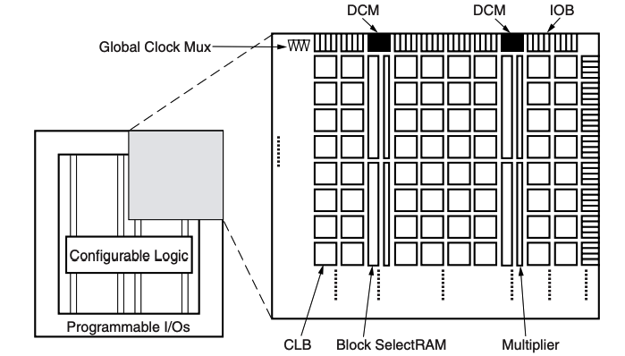
Arranged as a rectangular fabric, the internal layout consists of repeated columns of configurable logic blocks forming the main logic array, with dedicated vertical columns of block SelectRAM and hardware multipliers placed at regular intervals to support memory storage and arithmetic operations. Input and output blocks line the outer edges of the structure, providing programmable connections between internal logic and external pins. Digital clock manager blocks are positioned near the top edge and interface with global clock multiplexers and routing networks that span the device, enabling synchronized clock distribution across logic, memory, and multiplier resources. The organization reflects a balanced distribution of programmable logic, embedded resources, and clocking infrastructure within the FPGA.
IOB Block of XC2V500-5FGG456C
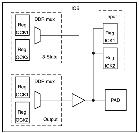
Structured around a single I/O pad, the block integrates separate input and output paths with six internal storage registers that support flexible data capture and launch. Two input registers labeled ICK1 and ICK2 allow incoming signals to be sampled on different clock edges, enabling double data rate operation. On the output side, paired registers OCK1 and OCK2 feed a DDR multiplexer that selects data based on clocking, followed by a three state control stage that manages output enable behavior. The shared internal routing connects both input and output logic to the pad, allowing the block to be configured for input, output, or bidirectional operation while supporting registered and DDR signaling modes.
Applications of XC2V500-5FGG456C
Embedded Digital Systems
The XC2V500-5FGG456C is used in embedded digital systems that require flexible logic for control, monitoring, and data coordination. Its programmable structure allows system functions to be adjusted or expanded without hardware changes, supporting long product lifecycles.
Industrial Automation and Control Equipment
In industrial control platforms, the device supports timing control, signal sequencing, and data handling tasks. It helps manage interactions between sensors, actuators, and controllers, allowing stable operation in systems that run continuously.
Telecommunications Infrastructure Hardware
Telecommunications equipment uses the device to manage data routing, protocol handling, and interface coordination. Its logic capacity supports parallel processing paths that help maintain steady data flow in network hardware.
Aerospace and Defense Electronic Systems
The device is applied in aerospace and defense electronics where predictable logic behavior and structured signal control are required. It supports processing and control functions in systems that operate under defined environmental and reliability standards.
Medical Diagnostic and Monitoring Equipment
In medical devices, the XC2V500-5FGG456C supports data acquisition, control logic, and signal coordination. Its programmable nature allows system designers to tailor functionality to specific monitoring and diagnostic requirements.
Automotive Electronics and Control Modules
Automotive control modules use the device for signal management, control sequencing, and data processing tasks. It supports integration of multiple control functions within a single programmable platform, helping reduce component count.
XC2V500-5FGG456C Advantages and Disadvantages
Advantages
• High logic density supports complex digital control and data handling
• Large on chip memory allows internal data buffering and temporary storage
• Reconfigurable structure supports reuse across different system designs
• High number of input and output pins enables connection to multiple interfaces
• Stable and well characterized architecture supports predictable operation
Disadvantages
• Higher power use compared with more recent programmable logic devices
• Limited compatibility with modern high speed interface standards
• Larger physical footprint compared with newer low power alternatives
• Development environment differs from current programmable logic platforms
XC2V500-5FGG456C Alternatives
| Part Number | Manufacturer | Key Features | Use Case/Notes |
| XC2V500-5FGG256C | AMD Xilinx | Virtex-II FPGA with around 500k system gates, moderate logic density, and balanced I/O count, offered in a compact FGG256 BGA package. | Suitable for mid-range FPGA designs where board space is limited, such as embedded processing, industrial control, and communication interfaces. |
| XC2V500-4FGG456C | AMD Xilinx | Virtex-II FPGA with a larger FGG456 package, providing higher I/O availability and a slower speed grade optimized for stable operation. | Well suited for applications needing many external connections, such as data acquisition systems, interface expansion, and control logic. |
| XC2V500-5FGG456I | AMD Xilinx | Industrial-grade Virtex-II FPGA with extended temperature support, higher speed grade, and a high-pin-count FGG456 package. | Designed for harsh-environment and long-life systems, including industrial automation, transportation electronics, and rugged control platforms. |
About Xilinx
Xilinx is a technology company known for developing programmable logic solutions used across a wide range of electronic systems. The company built its reputation around field programmable gate arrays and related devices that allow hardware behavior to be defined and updated through configuration rather than fixed circuitry. Its product portfolio has supported applications in communications, computing, industrial systems, and embedded platforms. Xilinx has focused on providing scalable logic platforms, long product lifecycles, and consistent design ecosystems that help system developers adapt hardware designs as requirements evolve.
Conclusion
The XC2V500-5FGG456C gives you a balanced mix of logic capacity, memory, and I/O flexibility in a single programmable device. Its Virtex-II architecture supports parallel processing and stable signal handling across many applications. You can use it to combine control, data movement, and interface tasks without adding extra chips. The BGA package helps keep board layouts compact while still offering many connections. While newer devices offer lower power and faster interfaces, this FPGA remains a solid option for well-defined systems. It works best when you value predictable behavior and design flexibility.
Datasheet PDF
XC2V500-5FGG456C Datasheet:
About us
ALLELCO LIMITED
Read more
Quick inquiry
Please send an inquiry, we will respond immediately.
Frequently Asked Questions [FAQ]
1. What type of device is the XC2V500-5FGG456C?
It is a field-programmable gate array that lets you configure digital logic functions through programming rather than fixed hardware.
2. How many I/O pins does the XC2V500-5FGG456C provide?
The device offers up to 264 programmable input and output pins for connecting external signals.
3. What package does the XC2V500-5FGG456C use?
It comes in a 456-ball fine-pitch BGA package designed for surface-mount assembly.
4. What kinds of systems commonly use this FPGA?
You often see it in embedded systems, industrial control equipment, telecom hardware, and other platforms needing flexible logic.
5. Who manufactures the XC2V500-5FGG456C?
It is produced by Xilinx, a well-known supplier of programmable logic devices.
PCB vs PCBA: What’s the Difference and Why it Matters in Electronics
on December 24th
Understanding the AD5328BRU 12-Bit Digital to Analog Converter
on December 23th
Popular Posts
-

Complex Instruction Set Computers: How They Changed Computing?
on April 18th 147778
-

USB-C Pinout and Features
on April 18th 112032
-

Using Xilinx Unified Simulation Primitives: A Comprehensive Guide to FPGA Design and Simulation
on April 18th 111351
-

Power Supply Voltages in Electronics: Meaning of VCC, VDD, VEE, VSS, and GND
on April 18th 83788
-

RJ45 Connector Guide: Pinout, Wiring, Cable Types, and Uses
on January 1th 79596
-

The Ultimate Guide to Wire Color Codes in Modern Electrical Systems
The way our electrical systems use colors isn’t just for looks. Each wire color now indicates a specific function, making it easier to identify and handle electrical components correctly during ins...on January 1th 66973
-

Purge Valve Guide: Function, Symptoms, Testing, and Replacement for Optimal Engine Performance
The purge valve is a key part of a car’s system that helps keep the air clean by managing fuel vapors before they can escape into the atmosphere. This not only helps the environment by reducing pol...on January 1th 63110
-

Quality (Q) Factor: Equations and Applications
The quality factor, or 'Q', is important when checking how well inductors and resonators work in electronic systems that use radio frequencies (RF). 'Q' measures how well a circuit minimizes energy...on January 1th 63043
-

Achieving Peak Performance with the Maximum Power Transfer Theorem
The Maximum Power Transfer Theorem explains how energy from a source, such as a battery or generator, flows to a connected load. It shows the exact condition where the load receives the most power....on January 1th 54097
-

A23 Battery Specifications and Compatibility
The A23 battery is a small, cylinder-shaped battery with high voltage. Also called 23A, 23AE, or MN21, it runs at 12 volts and much higher than AA or AAA batteries. Its special design make...on January 1th 52195
HOT Part Number
-

74HC4051DB,118
NXP USA Inc.
IC MUX/DEMUX 8X1 16SSOP
KSZ8895MQXI
Microchip Technology
IC ETHERNET SWITCH 5PORT 128PQFP
74F32PC
onsemi
IC GATE OR 4CH 2-INP 14DIP
TSOP34138
Vishay Semiconductor Opto Division
SENSOR REMOTE REC 38.0KHZ 45M
DAC7802KP
Texas Instruments
IC DAC 12BIT A-OUT 24DIP
IR21531STR
Infineon Technologies
IC GATE DRVR HALF-BRIDGE 8SOIC
BZG05C5V1-HM3-08
Vishay General Semiconductor - Diodes Division
DIODE ZENER 5.1V 1.25W DO214AC
HSMG-C265
Broadcom Limited
LED GREEN DIFFUSED CHIP SMD
EPM7128BFC256-4
Altera
IC CPLD 128MC 4NS 256FBGA
N25Q032A13E1241E
Micron Technology Inc.
IC FLASH 32MBIT SPI 24TPBGA
NCP18WM224J03RB
Murata Electronics
THERM NTC 220KOHM 4500K 0603
MCR100-004
onsemi
SCR 200V 800MA TO92-3
MADP-007448-0287BT
MACOM Technology Solutions
DIODE,PIN,PLASTIC,ST,LEADFREE
MAX6693UP9A+
Analog Devices Inc./Maxim Integrated
SENSOR DIGITAL -40C-125C 20TSSOP
Q8008LH4
Littelfuse Inc.
TRIAC ALTERNISTOR 800V 8A TO220
LM358PT
STMicroelectronics
IC OPAMP GP 2 CIRCUIT 8TSSOP
CL31C332JHHNNNE
Samsung Electro-Mechanics
CAP CER 3300PF 630V C0G/NP0 1206
LM339N
Fairchild Semiconductor
IC COMPARATOR 4 GEN PUR 14DIP -

MAX691EPE+
Analog Devices Inc./Maxim Integrated
IC SUPERVISOR 1 CHANNEL 16DIP
HMK432BJ105MM-T
Taiyo Yuden
CAP CER 1UF 100V X5R 1812
06035A131FA16A
KYOCERA AVX
CAP CER 130PF 50V C0G/NP0 0603
STF826
STMicroelectronics
TRANS PNP 30V 3A SOT89-3
P0900SALRP
Littelfuse Inc.
THYRISTOR 75V 150A DO214AA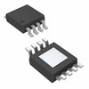
MP24875DN-LF-Z
Monolithic Power Systems Inc.
IC LED DRV RGLTR PWM 1.5A 8SOICE
TPS79501DRBR
Texas Instruments
IC REG LINEAR POS ADJ 500MA 8SON
TEA1755LT/1Y
NXP USA Inc.
IC OFFLINE SWITCH FLYBACK 16SO
AB-RTCMC-32.768KHZ-AIGZ-S7-T
Abracon LLC
IC RTC CLK/CALENDAR I2C 8CLCC
C1005X5R1H331M050BA
TDK Corporation
CAP CER 330PF 50V X5R 0402
RP115L181B-E2
Nisshinbo Micro Devices Inc.
IC REG LINEAR 1.8V 1A DFN1216-8
BZX384C3V6-E3-08
Vishay General Semiconductor - Diodes Division
DIODE ZENER 3.6V 200MW SOD323
CY7C027V-20AXC
Cypress Semiconductor Corp
IC SRAM 512KBIT PARALLEL 100TQFP
ADS7952SBDBTR
Texas Instruments
IC ADC 12BIT SAR 38TSSOP
A8904SLPTR-T
Allegro MicroSystems
IC MOTOR DRVR 4.5V-5.5V 28TSSOP
HIN241IA
Intersil
RS-232 TRANSMITTER/RECIEVER
122NQ030R
Vishay General Semiconductor - Diodes Division
DIODE SCHOTTKY 30V 120A D-67
ADC084S101CIMMX
Texas Instruments
IC ADC 8BIT SAR 10VSSOP -

MAT01GHZ
Analog Devices Inc.
TRANS 2NPN 45V 0.025A TO78-6
ADP5075ACBZ-R7
Analog Devices Inc.
IC REG BCK BST INV 800MA 12WLCSP
AON7200
Alpha & Omega Semiconductor Inc.
MOSFET N-CH 30V 15.8A/40A 8DFN
MMSZ5254B
Diotec Semiconductor
ZENER SOD-123 27V 0.5W 5%
1N1301
Solid State Inc.
DIODE GEN PURP 50V 40A DO5
CC0805ZRY5V9BB224
YAGEO
CAP CER 0.22UF 50V Y5V 0805
LM709CH
Texas Instruments
IC OPAMP GP 1 CIRCUIT TO99-8
LCB111STR
IXYS Integrated Circuits Division
SSR RELAY SPST-NC 120MA 0-350V
LMV821M5X
Texas Instruments
IC OPAMP GP 1 CIRCUIT SOT23-5
2N5330
Microchip Technology
POWER BJT
E0505S-1WR3
Mornsun America, LLC
DC DC CONVERTER +/-5V 1W
1-320551-4
TE Connectivity AMP Connectors
CONN RING CIRC 18AWG #8 CRIMP
TOP243PN
Power Integrations
IC OFFLINE SWITCH FLYBACK 8DIP
MC9S12DG256BMPV
NXP USA Inc.
IC MCU 16BIT 256KB FLASH 112LQFP
SMF48A
Diotec Semiconductor
TVS SOD-123FL 48V 200W UNI
BCM88770A1KFSBG
Broadcom Limited
144 SERDES MULTI STAGE
1N4762A-TAP
Vishay General Semiconductor - Diodes Division
DIODE ZENER 82V 1.3W DO41
SIT9121AI-2D2-33E200.000000
SiTime
MEMS OSC XO 200.0000MHZ LVDS SMD