
 AD8609ARUZ-REELAnalog Devices Inc.IC CMOS 4 CIRCUIT 14TSSOP
 AD8608ARUZ-REELAnalog Devices Inc.IC CMOS 4 CIRCUIT 14TSSOP
 AD8608ARUZAnalog Devices Inc.IC CMOS 4 CIRCUIT 14TSSOP
 AD8608ARU-REELAnalog Devices Inc.IC OPAMP GP R-R CMOS 14TSSOP
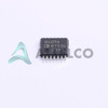 AD8609ARUZAnalog Devices Inc.IC CMOS 4 CIRCUIT 14TSSOP
 AD8608ARZAnalog Devices Inc.IC CMOS 4 CIRCUIT 14SOIC
 AD8608ARZ-REEL7Analog Devices Inc.IC CMOS 4 CIRCUIT 14SOIC
 AD8609
- Dani***alkerTech
- Jun 1, 2026
HomeProductsIntegrated Circuits (ICs)Linear - Amplifiers - Instrumentation, OP Amps, Buffer AmpsAD8609AR

Image may be representation.
See specifications for product details.
See specifications for product details.
- EXPRESS OPTION
- Payment method
AD8609AR - Analog Devices Inc.
- Manufacturer Part Number
- AD8609AR
- Manufacturer
- Analog Devices, Inc.
- Allelco Part Number
- 98D-AD8609AR
- Warranty
- 1 Year Allelco Warranty - Find out more
- Stock Status:
- 14,302 pcs available, New & Original
- Parts Description
- IC OPAMP GP R-R CMOS QUAD 14SOIC
- Package
- 14-SOIC
- Data sheet
-
AD8609AR.pdf
Datasheets
AD8603,07,09.pdfPCN Obsolescence/ EOL
Multiple Device Family 05/Oct/2010.pdf
- RoHs Status
- Our certification
- In stock: 14302


