
 LCMXO2-4000HC-4FTG256CLattice Semiconductor CorporationIC FPGA 206 I/O 256FTBGA
 LCMXO2-4000HC-4QN84CLattice Semiconductor CorporationIC FPGA 68 I/O 84QFN
 LCMXO2-4000HC-4BG332CLattice Semiconductor CorporationIC FPGA 274 I/O 332CABGA
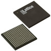 LCMXO2-4000HC-4BG256CLattice Semiconductor CorporationIC FPGA 206 I/O 256CABGA
 LCMXO2-256ZE-3UMG64ILattice Semiconductor CorporationIC FPGA 44 I/O 64UCBGA
 LCMXO2-4000HC-4MG132CLattice Semiconductor CorporationIC FPGA 104 I/O 132CSBGA
- Nath***rooks
- Jun 11, 2026
HomeProductsIntegrated Circuits (ICs)Embedded - FPGAs (Field Programmable Gate Array)LCMXO2-4000HC-4FG484I
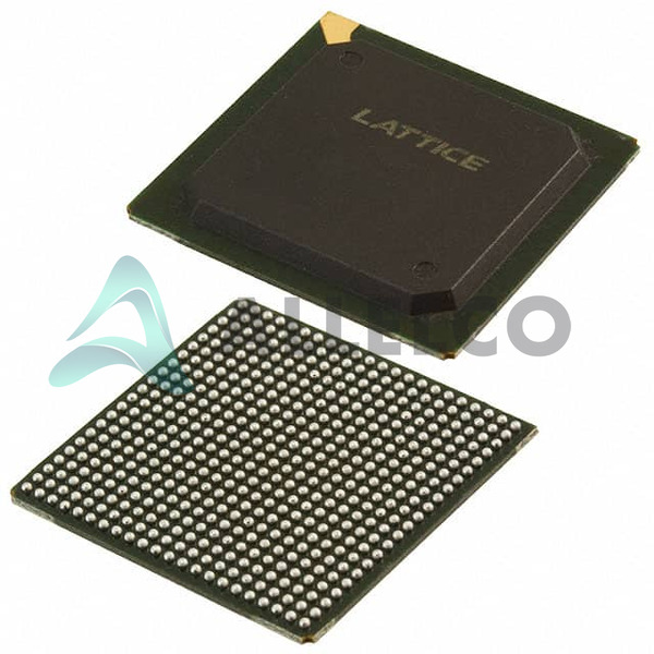
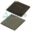
Image may be representation.
See specifications for product details.
See specifications for product details.
- EXPRESS OPTION
- Payment method
LCMXO2-4000HC-4FG484I - Lattice Semiconductor Corporation
- Manufacturer Part Number
- LCMXO2-4000HC-4FG484I
- Manufacturer
- Lattice Semiconductor
- Allelco Part Number
- 98D-LCMXO2-4000HC-4FG484I
- Warranty
- 1 Year Allelco Warranty - Find out more
- Stock Status:
- 31,821 pcs available, New & Original
- Parts Description
- IC FPGA 278 I/O 484FBGA
- Package
- 484-FBGA (23x23)
- Data sheet
-
LCMXO2-4000HC-4.pdf
Getting Started Guide
Product Selector Guide.pdfPCN Other
I2C Read-Back Failure Feb/2015.pdfPCN Packaging
All Dev Pkg Mark Chg 12/Nov/2018.pdfPCN Assembly/Origin
Alternate Qualified Test Site 30/Sep/2013.pdf
- RoHs Status
- ROHS3 Compliant
- Our certification
- In stock: 31821
- Unit Price: $31.95
- Subtotal: $0.00
Want a better price?
Add to Cart and Submit RFQ now, we'll contact you immediately.
| Quantity | Unit Price | Ext. Price |
|---|---|---|
| 1+ | $31.95 | $31.95 |
The above prices does not include taxes and freight rates, which will be calculated on the order pages.


