View All

Please refer to the English Version as our Official Version.Return

Europe
France(Français) Germany(Deutsch) Italy(Italia) Russian(русский) Poland(polski) Czech(Čeština) Luxembourg(Lëtzebuergesch) Netherlands(Nederland) Iceland(íslenska) Hungarian(Magyarország) Spain(español) Portugal(Português) Turkey(Türk dili) Bulgaria(Български език) Ukraine(Україна) Greece(Ελλάδα) Israel(עִבְרִית) Sweden(Svenska) Finland(Svenska) Finland(Suomi) Romania(românesc) Moldova(românesc) Slovakia(Slovenská) Denmark(Dansk) Slovenia(Slovenija) Slovenia(Hrvatska) Croatia(Hrvatska) Serbia(Hrvatska) Montenegro(Hrvatska) Bosnia and Herzegovina(Hrvatska) Lithuania(lietuvių) Spain(Português) Switzerland(Deutsch) United Kingdom(English)
Asia/Pacific
Japan(日本語) Korea(한국의) Thailand(ภาษาไทย) Malaysia(Melayu) Singapore(Melayu) Vietnam(Tiếng Việt) Philippines(Pilipino)
Africa, India and Middle East
United Arab Emirates(العربية) Iran(فارسی) Tajikistan(فارسی) India(हिंदी) Madagascar(malaɡasʲ)
South America / Oceania
New Zealand(Maori) Brazil(Português) Angola(Português) Mozambique(Português)
North America
United States(English) Canada(English) Haiti(Ayiti) Mexico(español)
HomeProductsIntegrated Circuits (ICs)Embedded - FPGAs (Field Programmable Gate Array)LCMXO2-4000HC-4TG144I
LCMXO2-4000HC-4TG144I Image
Image may be representation.
See specifications for product details.
EXPRESS OPTION
Payment method

LCMXO2-4000HC-4TG144I - Lattice Semiconductor Corporation

Manufacturer Part Number
LCMXO2-4000HC-4TG144I
Manufacturer
Lattice Semiconductor
Allelco Part Number
32D-LCMXO2-4000HC-4TG144I
Warranty
1 Year Allelco Warranty - Find out more
Stock Status:
2,096 pcs available, New & Original
Parts Description
IC FPGA 114 I/O 144TQFP
Package
144-TQFP (20x20)
Data sheet
LCMXO2-4000HC-4.pdf
RoHs Status
ROHS3 Compliant
Our certification
In stock: 2096
  • Unit Price: $6.153
  • Subtotal: $0.00

Want a better price?
Add to Cart and Submit RFQ now, we'll contact you immediately.

Quantity Unit Price Ext. Price
1+ $6.153 $6.15
10+ $5.04 $50.40
30+ $4.591 $137.73
100+ $4.215 $421.50
The above prices does not include taxes and freight rates, which will be calculated on the order pages.

Specifications

LCMXO2-4000HC-4TG144I Tech Specifications
Lattice Semiconductor Corporation - LCMXO2-4000HC-4TG144I technical specifications, attributes, parameters and parts with similar specifications to Lattice Semiconductor Corporation - LCMXO2-4000HC-4TG144I

Product Attribute Attribute Value
Manufacturer Lattice Semiconductor
Voltage - Supply 2.375V ~ 3.465V
Total RAM Bits 94208
Supplier Device Package 144-TQFP (20x20)
Series MachXO2
Package / Case 144-LQFP
Package Tray
Product Attribute Attribute Value
Operating Temperature -40°C ~ 100°C (TJ)
Number of Logic Elements/Cells 4320
Number of LABs/CLBs 540
Number of I/O 114
Mounting Type Surface Mount
Base Product Number LCMXO2-4000

Environmental & Export Classifications

ATTRIBUTE DESCRIPTION
RoHs Status ROHS3 Compliant
Moisture Sensitivity Level (MSL) 3 (168 Hours)
REACH Status REACH Unaffected
ECCN EAR99
HTSUS 8542.39.0001

Parts Introduction

LCMXO2-4000HC-4TG144I Image
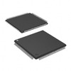
LCMXO2-4000HC-4TG144I (1)

Manufacturer Part Number

LCMXO2-4000HC-4TG144I

Manufacturer

Lattice Semiconductor

Introduction

The LCMXO2-4000HC-4TG144I is a MachXO2 series embedded FPGA, designed for low-density applications requiring flexible I/O interfacing with low power consumption.

Product Features and Performance

540 LABs/CLBs

4320 Logic Elements/Cells

94208 Total RAM Bits

114 Number of I/O

Voltage Supply Range: 2.375V to 3.465V

Surface Mount Technology

Temperature Tolerance: -40°C to 100°C

144-LQFP Packaging

Product Advantages

Optimized for low power applications

Highly flexible I/O interfacing

Robust temperature range making it suitable for harsh environments

Key Technical Parameters

Total Number of LABs/CLBs: 540

Total Logic Elements/Cells: 4320

Total RAM Bits: 94208

Number of Inputs/Outputs: 114

Voltage Supply Range: 2.375V to 3.465V

Maximum Operating Temperature: 100°C

Mounting Type: Surface Mount

Package Type: 144-LQFP

Quality and Safety Features

Operates efficiently within industrial temperature ranges

Compliant with standard surface mount technology requirements for safety

Compatibility

Compatible with various standard interfacing protocols, suited for mixed-signal operations

Application Areas

Consumer Electronics

Telecommunications Systems

Automotive Applications

Industrial Automation

Product Lifecycle

Active product status

Ongoing updates and support available

No current notice of discontinuation

Several Key Reasons to Choose This Product

Low power consumption suited for energy-sensitive projects

Highly configurable I/O for diverse application needs

Supports a wide range of operating temperatures, ensuring reliability in varying environmental conditions

Ongoing product lifecycle support from Lattice Semiconductor ensures long-term usability and updates

Frequently Asked Questions(FAQ)

How does the LCMXO2-4000HC-4TG144I compare to other MachXO2 variants in terms of logic density and power efficiency for low-power embedded applications?
The LCMXO2-4000HC-4TG144I offers 4320 logic elements and 94208 RAM bits, making it one of the higher-density members of the MachXO2 family. Compared to lower-end models like the LCMXO2-1200HC, which provides only 1728 logic cells, this variant delivers approximately 2.5x more logic capacity while maintaining the same 2.375V to 3.465V operating voltage range. Its hardened I²C and SPI interfaces reduce microcontroller overhead, contributing to better system-level power efficiency. However, the HC version trades off slightly higher static power consumption compared to the HE variant under similar workloads, so designers must balance performance needs with thermal constraints.
What are the key considerations when selecting between the LCMXO2-4000HC-4TG144I and alternative FPGA solutions for industrial temperature applications?
For industrial environments requiring operation from -40°C to +100°C, the LCMXO2-4000HC-4TG144I meets the full temperature range with TJ max of 100°C, unlike some consumer-grade FPGAs that may derate beyond 85°C. While it lacks the hardened transceivers found in larger FPGAs such as Xilinx Artix-7, its non-volatile configuration eliminates external memory, improving reliability in harsh conditions. When compared to CPLDs of equivalent logic size, it offers significantly more flexibility and scalability but consumes more power at idle. Designers should evaluate boot time, I/O count (114 pins), and available LABs (540) against application requirements before finalizing selection.
Can the LCMXO2-4000HC-4TG144I be used in automotive systems, and what limitations apply given its RoHS and qualification status?
The LCMXO2-4000HC-4TG144I is not qualified to AEC-Q100 standards, limiting its direct use in safety-critical automotive subsystems such as ADAS or engine control. It is RoHS3 compliant and REACH unaffected, supporting environmental regulations common in European markets, but lacks the extended temperature grades and fault tolerance required for most automotive classes. It may find limited use in infotainment or body electronics where functional safety is not mandated, provided the system operates within -40°C to +100°C and avoids high-reliability requirements.
How does the Moisture Sensitivity Level (MSL) of 3 for the LCMXO2-4000HC-4TG144I impact PCB assembly and storage practices?
With an MSL rating of 3, the LCMXO2-4000HC-4TG144I has a floor life of up to 168 hours at 30°C/60% RH before reflow soldering. After opening the moisture-barrier bag, it must be stored in a dry environment or re-bagged with desiccant and humidity indicator cards. If exposed beyond this window without baking, popcorning during reflow can damage the package. Manufacturers typically recommend baking only if humidity indicators show exposure, as excessive baking may compromise solder joint integrity. Proper handling reduces risk in high-volume production.
What trade-offs exist between using the LCMXO2-4000HC-4TG144I versus discrete logic components for glue logic functions in embedded systems?
Replacing discrete logic gates with the LCMXO2-4000HC-4TG144I allows integration of complex state machines, protocol translation, and timing control into a single device, reducing board space and BOM count. However, each logic cell consumes static current—typically around 1–2 mA per 1000 LEs under typical conditions—leading to higher standby power than dedicated ICs. The benefit becomes clear in designs requiring >500 gates of programmable logic, where the FPGA’s built-in I/O buffers and slew rate control simplify interfacing compared to cascaded TTL or CMOS parts.
How does the total RAM bit count of 94208 in the LCMXO2-4000HC-4TG144I influence data buffering and FIFO design compared to smaller MachXO2 variants?
With 94208 bits of distributed and block RAM, the LCMXO2-4000HC-4TG144I supports large dual-port FIFOs or lookup tables that exceed the capacity of smaller MachXO2 devices like the -1200HC (18432 bits). This enables efficient packet buffering in Ethernet or USB applications without external SRAM. However, RAM allocation competes with logic resources; allocating 32K bits to a FIFO may reduce available LABs by ~15%, affecting routing congestion. Designers must model resource usage early to avoid timing closure issues.
In what scenarios would the hardened I²C and SPI blocks in the LCMXO2-4000HC-4TG144I provide significant advantages over software-driven implementations on a microcontroller?
The LCMXO2-4000HC-4TG144I includes dedicated hardened I²C and SPI peripherals that offload timing-critical communication tasks from the main processor. This reduces CPU load, minimizes jitter, and ensures deterministic response times in real-time systems such as sensor networks or motor controllers. Unlike soft IP, these blocks handle arbitration, clock stretching, and multi-master protocols automatically. For applications requiring multiple simultaneous serial links—such as connecting several sensors via I²C—using the FPGA’s native blocks simplifies firmware development and improves system reliability.
How does the 114 I/O capability of the LCMXO2-4000HC-4TG144I affect pin planning and signal integrity when migrating from a CPLD-based design?
The LCMXO2-4000HC-4TG144I’s 114 general-purpose I/Os allow greater flexibility than many CPLDs but require careful assignment to avoid bank conflicts due to voltage domain restrictions. Each I/O bank operates within the 2.375V–3.465V supply window, so mixed-voltage interfaces must use level shifters unless both sides are within spec. With 144-pin TQFP packaging, thermal dissipation is manageable, but high-speed signals should follow length-matching rules and avoid adjacent vias to minimize crosstalk. Careful placement in the PCB layout phase prevents routing congestion and ensures compliance with setup/hold times.
What is the impact of the LCMXO2-4000HC-4TG144I’s non-volatile configuration on system boot-up time and reliability compared to SRAM-based FPGAs?
Since the LCMXO2-4000HC-4TG144I stores configuration internally and powers up immediately without external flash, it achieves faster boot times than volatile SRAM-based FPGAs, which require serial flash read cycles at startup. This enhances system availability in always-on applications. Additionally, there is no external configuration memory to fail or degrade over time, increasing long-term reliability. However, reprogramming requires ISP (In-System Programming) via JTAG, whereas some SRAM FPGAs support remote updates—this limits field upgradability depending on application needs.
Why might a designer choose the LCMXO2-4000HC-4TG144I instead of an ASIC for a medium-volume embedded control application?
For volumes between 1k and 10k units, the LCMXO2-4000HC-4TG144I offers faster time-to-market and lower NRE costs compared to custom ASICs, while providing sufficient logic (4320 LEs) and I/O for many control tasks. Unlike ASICs, it supports rapid prototyping and iterative development. Although unit cost remains above CPLDs, it avoids mask expenses and allows reuse across product lines. Only if extreme power efficiency (<1mW) or ultra-low cost per unit is required would an ASIC become justified—otherwise, the FPGA’s flexibility dominates the decision.
How does the operating temperature range of -40°C to +100°C for the LCMXO2-4000HC-4TG144I affect derating guidelines for continuous high-load operation?
Operating continuously at 100°C TJ stresses the device near its maximum rating, necessitating conservative thermal design. Power dissipation should be derated to stay well below typical junction-to-ambient thermal resistance values (e.g., <1.5W for most LQFP packages). In enclosures with poor airflow, ambient temperature must be kept below 70°C even if the FPGA runs cooler. Thermal vias under the package and strategic copper pours improve heat spreading. Monitoring die temperature via internal sensors (if available) helps prevent thermal runaway in fault conditions.
What are the implications of the LCMXO2-4000HC-4TG144I’s ECCN classification (EAR99) for international export compliance?
Classified under ECCN EAR99, the LCMXO2-4000HC-4TG144I is generally subject to U.S. Commerce Control List (CCL) Category 3 controls but is often eligible for License Exception ENC or LVS when exported to most countries. However, end-use restrictions may apply if intended for military, surveillance, or proliferation-sensitive applications. Exporters should verify destination country regulations and end-user status, as misclassification could lead to compliance violations. Always consult current BIS guidelines before shipping internationally.
How does the number of LABs (540) in the LCMXO2-4000HC-4TG144I influence synthesis strategy and routing complexity in larger designs?
With 540 LABs organized into columns, the LCMXO2-4000HC-4TG144I supports moderately complex designs but requires careful partitioning to avoid routing congestion. LABs share local interconnect, so tightly coupled logic should be grouped together. Synthesis tools benefit from specifying timing constraints early, especially for paths crossing LAB boundaries. Poorly constrained designs may fail place-and-route despite fitting logically, as global routing delays increase nonlinearly near I/O banks. Using incremental compilation and floorplanning can mitigate these effects in multi-module projects.
Can the LCMXO2-4000HC-4TG144I support LVDS signaling, and what precautions are needed for high-speed differential pairs?
The LCMXO2-4000HC-4TG144I does not include hardened LVDS transceivers, so differential signaling must be implemented using soft logic. While possible, achieving reliable 600 Mbps+ performance demands matched traces, controlled impedance routing, and careful skew management. Soft LVDS consumes more power and area than hardened versions and lacks built-in termination. For applications requiring true LVDS, consider external serializer/deserializer chips or migrate to a device with native SERDES. Otherwise, LVPECL or HCSL may offer better performance margins.
How does the package choice (TQFP vs. BGA) affect reworkability and yield when working with the LCMXO2-4000HC-4TG144I?
The 144-TQFP (20x20 mm) package uses fine-pitch leads that are more reworkable than BGA alternatives, allowing hand-soldering or standard pick-and-place repair under magnification. However, pin count limits further miniaturization, and solder bridging risks increase with hand assembly. Automated production yields remain high due to mature SMT processes, but inspection (AOI or X-ray) is recommended for joints near center. Migration to BGA would reduce board area but complicate debugging and replacement, making TQFP preferable for prototyping and moderate-volume designs.
What role does the hardened USB interface play in differentiating the LCMXO2-4000HC-4TG144I from other MachXO2 devices, and how does it impact system integration?
The presence of a hardened USB 2.0 Full-Speed interface in the LCMXO2-4000HC-4TG144I distinguishes it from basic MachXO2 models without USB support, enabling direct host or peripheral functionality without external PHY chips. This simplifies USB stack implementation and reduces component count in embedded gateways or data loggers. The block handles enumeration, packet framing, and handshake protocols automatically, freeing firmware developers from low-level USB compliance details. However, it occupies fixed logic resources and cannot be repurposed for other functions, so its inclusion must align with target connectivity requirements.
How does the absence of hardened transceivers in the LCMXO2-4000HC-4TG144I influence choices for high-speed serial communication compared to larger FPGAs?
Without hardened transceivers, the LCMXO2-4000HC-4TG144I cannot support native Gigabit Ethernet, PCIe, or DDR3 interfaces common in larger FPGAs. Instead, designers must implement serial protocols using soft IP or external PHYs, limiting maximum data rates to USB 2.0 Full Speed (~12 Mbps) or custom Manchester-coded links. While adequate for control-oriented applications, this restricts use in video processing or high-bandwidth networking. For such cases, pairing the FPGA with companion PHYs increases BOM cost and board complexity, making alternatives like CPLDs or ASSPs more suitable unless future scalability justifies the FPGA investment.
What design considerations arise from the LCMXO2-4000HC-4TG144I’s voltage tolerance window of 2.375V to 3.465V when interfacing with legacy 3.3V or 5V systems?
The LCMXO2-4000HC-4TG144I operates safely at 3.3V but not at 5V, so direct connection to 5V TTL or RS-232 levels risks damaging inputs unless clamped appropriately. Level shifting is required when communicating with 5V logic families. At 2.375V, noise margins decrease, potentially violating input thresholds in noisy environments. Designers should ensure VOH/VOL specifications meet receiver requirements across all operating voltages. Decoupling capacitors and series resistors on critical lines help stabilize signals, and ESD protection diodes add robustness during hot-plug events.

Parts with Similar Specifications

The three parts on the right have similar specifications to Lattice Semiconductor Corporation LCMXO2-4000HC-4TG144I

Product Attribute LCMXO2-4000HC-4TG144C LCMXO2-4000HC-4FG484I LCMXO2-4000HC-4MG132I LCMXO2-4000HC-4FTG256I
Part Number LCMXO2-4000HC-4TG144C LCMXO2-4000HC-4FG484I LCMXO2-4000HC-4MG132I LCMXO2-4000HC-4FTG256I
Manufacturer Lattice Semiconductor Corporation Lattice Semiconductor Corporation Lattice Semiconductor Corporation Lattice Semiconductor Corporation
Number of Logic Elements/Cells - - - -
Supplier Device Package - 196-NFBGA (12x12) 16-PDIP 64-VQFN (9x9)
Mounting Type - Surface Mount Through Hole Surface Mount
Number of I/O - - - -
Number of LABs/CLBs - - - -
Package - Tape & Reel (TR) Tube Tape & Reel (TR)
Package / Case - 196-LFBGA 16-DIP (0.300', 7.62mm) 64-VFQFN Exposed Pad
Voltage - Supply - - - -
Operating Temperature - -40°C ~ 85°C 0°C ~ 70°C -40°C ~ 85°C
Total RAM Bits - - - -
Base Product Number - DAC34H84 MAX500 ADS62P42
Series - - - -

LCMXO2-4000HC-4TG144I Datasheet PDF

Download LCMXO2-4000HC-4TG144I pdf datasheets and Lattice Semiconductor Corporation documentation for LCMXO2-4000HC-4TG144I - Lattice Semiconductor Corporation.

Datasheets
MachXO2 Family Datasheet.pdf
PCN Packaging
All Dev Pkg Mark Chg 12/Nov/2018.pdf
PCN Assembly/Origin
Alternate Assembly Revision B 17/Nov/2014.pdf
Manuals
Leaded Pkg PCB Layout Guide.pdf
PCN Design/Specification
MachXO2 Family Datasheet 30/Sep/2013.pdf QFP Dev Marking Chgs 28/Sep/2020.pdf

Customer Reviews

Evaluation: 10 Articles

  • Nath***rooks
    Jun 11, 2026

    Installed this power component in a converter board. Output remained stable under different load conditions and thermal performance was better than expected.

  • Dani***alkerTech
    Jun 1, 2026

    Product works, but setup took more effort than expected. Once configured the MCU ran reliably, although documentation support felt older compared with newer platforms. Fine for maintenance projects.

  • Yuki***aka88
    May 26, 2026

    信号通信プロジェクトでこのRS-485トランシーバーを使用しました。設置は簡単で、長距離ケーブルでも通信は安定していました。消費電力も、以前使用していたものより低くなっています。

  • Stev***aker
    May 20, 2026

    Solid diode for power rectification. Works well in switching circuits.

  • Bran***Lewis
    May 11, 2026

    Compact FPGA with good performance. Suitable for basic signal processing tasks.

  • Oliv***arris
    May 7, 2026

    Reliable I/O expander. Works well in embedded control applications.

  • Jess***Jones
    Apr 17, 2026

    It offers good value for the price, and the specifications match the description. I’ve been using it for two days with no issues, and I’ll definitely buy it again if I need it in the future.

  • Mich***Smith
    Apr 17, 2026

    Shipping was on time, the component pins are neatly aligned, and I tested 10 of them with a multimeter—all readings were within the specified range. Highly recommended.

  • Aman***arris
    Apr 3, 2026

    It was great—the entire process, from placing the order to receiving the package, went very smoothly. The components were consistent, the price was fair, and I had a very pleasant shopping experience.

  • Mike***nch
    Apr 3, 2026

    Better than expected! The resistance and capacitance readings were spot-on, and it passed the test on the first try. The service was reliable, and the packaging was thoughtful—I highly recommend it.

Write a Review

Your Email address will not be published.

Shipment

Delivery Time

In-stock items can be shipped within 24 hours. Some parts will be arranged for delivery within 1-2 days from the date all items arrive at our warehouse. And Allelco ships order once a day at about 17:00, except Sunday. Once the goods are shipped, the estimated delivery time depends on the shipping methods and Delivery destination. The table below shows are the logistic time for some common countries.

Delivery Cost

  1. Use your express account for shipment if you have one.
  2. Use our account for the shipment. Refer to the table below for the approximate charges.
(Different time frame / countries / package size has different price.)

Delivery Method

  1. Global Common Shipment by DHL / UPS / FedEx / TNT / EMS / SF we support.
  2. Others more shipping ways, please get in touch with your customer manager.

Common Countries Logistic Time Reference
Region Country Logistic Time(Day)
America United States 5
Brazil 7
Europe Germany 5
United Kingdom 4
Italy 5
Oceania Australia 6
New Zealand 5
Asia India 4
Japan 4
Middle East Israel 6
DHL & FedEx Shipment Charges Reference
Shipment charges(KG) Reference DHL(USD$)
0.00kg-1.00kg USD$30.00 - USD$60.00
1.00kg-2.00kg USD$40.00 - USD$80.00
2.00kg-3.00kg USD$50.00 - USD$100.00
Note:
The above table is for reference only. There may have some data bias for the uncontrollable factors.
Contact us if you have any questions.
  • QC (Quality Warranty)
  • Payment Support
  • Packaging
  • Certifications & Memberships

QC (Quality Warranty)

Allelco is committed to exceeding customer expectations through customer service excellence, order accuracy, and on-time delivery.
This is achieved through our commitment to the continual improvement of our processes, services, and products.


Strict quality inspection builds a solid foundation for electronic component quality.
  1. Visual inspection
  2. Performance testing and reliability verification
  3. Standardized full-process testing
  4. Precise control of every parameter
We eliminate defective components and ensure the stable operation of electronic devices through professional quality standards.

Payment Support

The payment method can be chosen from the methods shown below: Wire Transfer (T/T, Bank Transfer), Western Union, Credit card, PayPal.
  • HKBea
  • Paypal
  • MasterCard
  • Western-Union
  • VISA
Stable Delivery, Sincere Partnership — Your Faithful Supply Chain Partner
  • Efficient Supply Management
  • Cost-Saving Procurement
  • Fast Sourcing & Delivery
Contact us if you have any questions.

Packaging

Electrostatic Discharge Protection and Handling

All electrostatic-sensitive components are handled in accordance with electrostatic discharge control procedures. The products are hermetically sealed in anti-static safe packaging to prevent electrostatic damage. Appropriate labeling is also applied for identification and traceability. This ensures product integrity during storage, handling and transportation.


ESD

Certifications & Memberships

Third-party certified, strict quality control. Our certification
  • ISO 9001: 2015
  • ISO 13485: 2016
  • ISO 14001: 2015
  • ISO 28000: 2007
  • ISO 45001: 2018
  • GB/T 27922-2011
  • SMTA
  • IPC
  • ESD
  • PSMA
LCMXO2-4000HC-4TG144I Image

LCMXO2-4000HC-4TG144I

Lattice Semiconductor Corporation
32D-LCMXO2-4000HC-4TG144I

Want a better price? Add to Cart and Submit RFQ now, we'll contact you immediately.

0 RFQ
Shopping cart (0 Items)
It is empty.
Compare List (0 Items)
It is empty.
Feedback

Your feedback matters! At Allelco, we value the user experience and strive to improve it constantly.
Please share your comments with us via our feedback form, and we'll respond promptly.
Thank you for choosing Allelco.

Subject
E-mail
Comments
Captcha
Drag or click to upload file
Upload File
types: .xls, .xlsx, .doc, .docx, .jpg, .png and .pdf.
Max file size: 10MB