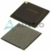
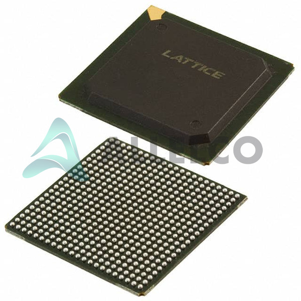
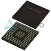
LCMXO2-4000HC-5FG484I (1)
Manufacturer Part Number
LCMXO2-4000HC-5FG484I
Manufacturer
Lattice Semiconductor
Introduction
The LCMXO2-4000HC-5FG484I is part of Lattice Semiconductor's MachXO2 series, which are Embedded FPGAs designed for versatile applications in various fields requiring programmable logic solutions.
Product Features and Performance
Embedded FPGA with 540 LABs/CLBs
Features 4320 Logic Elements/Cells
Offers a total RAM of 94208 bits
Provides 278 I/O pins for comprehensive connectivity options
Surface Mount package simplifies board design and manufacturing
Product Advantages
Efficient power consumption with a supply voltage range of 2.375V to 3.465V
Wide operating temperature range from -40°C to 100°C ensures reliability under varying environmental conditions
High-density package (484-BBGA) allows for compact board designs
Key Technical Parameters
Number of LABs/CLBs: 540
Number of Logic Elements/Cells: 4320
Total RAM Bits: 94208
Number of I/O: 278
Voltage Supply: 2.375V ~ 3.465V
Operating Temperature: -40°C ~ 100°C
Quality and Safety Features
Robust design suited for extended temperature operation
Manufactured in a high-integrated package for improved reliability
Compatibility
Compatible with surface mount technology for straightforward PCB integration
Application Areas
Ideal for communication infrastructure
Suitable for industrial applications, automotive systems, and consumer electronics
Product Lifecycle
Currently active with ongoing support and supply
Not nearing discontinuation, with viable options for upgrades available
Several Key Reasons to Choose This Product
High logic density supports complex digital systems
Flexible I/O count suitable for various integration requirements
Low power consumption aligns with energy-efficient design goals
Robust operational temperature range supports use in harsh environments
Reliable manufacturer with a history of delivering quality FPGA products
 LCMXO2-4000HC-5BG332ILattice Semiconductor CorporationIC FPGA 274 I/O 332CABGA
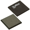 LCMXO2-4000HC-5BG256ILattice Semiconductor CorporationIC FPGA 206 I/O 256CABGA
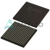 LCMXO2-4000HC-5FTG256CLattice Semiconductor CorporationIC FPGA 206 I/O 256FTBGA
 LCMXO2-4000HC-5MG132ILattice


