
LCMXO2-4000HC-5TG144I (1)
Manufacturer Part Number
LCMXO2-4000HC-5TG144I
Manufacturer
Lattice Semiconductor
Introduction
MachXO2-4000HC is a highly versatile, low power FPGA featuring programmable logic, I/O, and memory characteristics suitable for a variety of applications.
Product Features and Performance
Field Programmable Gate Array (FPGA)
High-count logic elements for complex designs
Extensive on-chip memory
High I/O count for peripheral connectivity
Support for a wide range of voltage supplies
Surface mount 144-LQFP packaging for compact integration
Operates effectively in extended temperatures from -40°C to 100°C
Product Advantages
Low power consumption suitable for power-sensitive applications
Rapid deployment of embedded design thanks to programmable nature
Reprogrammability for iterative development and updates
Dense logic capacity for a smaller footprint
Key Technical Parameters
Number of LABs/CLBs: 540
Number of Logic Elements/Cells: 4320
Total RAM Bits: 94208
Number of I/O: 114
Voltage Supply range: 2.375V to 3.465V
Operating Temperature range: -40°C to 100°C
Quality and Safety Features
Extended temperature range ensures reliability in various environments
Trusted manufacturer with a reputation for quality in FPGA products
Compatibility
Supports various standard logic levels for simplified interfacing
Surface Mount 144-LQFP package widely compatible with PCB designs
Application Areas
Industrial control systems
Consumer electronics
Automotive
Telecommunications
Embedded computing
Product Lifecycle
Active status indicating ongoing manufacture and support
Not approaching discontinuation at knowledge cutoff
Options for replacements or upgrades should be checked with Lattice Semiconductor
Several Key Reasons to Choose This Product
Energy-efficient FPGA suitable for battery-powered applications
Versatile device that can be used across various industries and applications
Capable of complex logic, memory, and processing tasks in a single chip
Improves time-to-market due to reprogrammability
Rugged design accommodating a wide range of operating conditions
Strong support and documentation from Lattice Semiconductor
Upgrade paths available to anticipate future technology needs
 LCMXO2-4000HC-6BG256CLattice Semiconductor CorporationIC FPGA 206 I/O 256CABGA
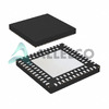 LCMXO2-4000HC-5QN84ILattice Semiconductor CorporationIC FPGA 68 I/O 84QFN
 LCMXO2-4000HC-6BG332ILattice Semiconductor CorporationIC FPGA 274 I/O 332CABGA
 LCMXO2-4000HC-6FTG256ILattice


