View All

Please refer to the English Version as our Official Version.Return

Europe
France(Français) Germany(Deutsch) Italy(Italia) Russian(русский) Poland(polski) Czech(Čeština) Luxembourg(Lëtzebuergesch) Netherlands(Nederland) Iceland(íslenska) Hungarian(Magyarország) Spain(español) Portugal(Português) Turkey(Türk dili) Bulgaria(Български език) Ukraine(Україна) Greece(Ελλάδα) Israel(עִבְרִית) Sweden(Svenska) Finland(Svenska) Finland(Suomi) Romania(românesc) Moldova(românesc) Slovakia(Slovenská) Denmark(Dansk) Slovenia(Slovenija) Slovenia(Hrvatska) Croatia(Hrvatska) Serbia(Hrvatska) Montenegro(Hrvatska) Bosnia and Herzegovina(Hrvatska) Lithuania(lietuvių) Spain(Português) Switzerland(Deutsch) United Kingdom(English)
Asia/Pacific
Japan(日本語) Korea(한국의) Thailand(ภาษาไทย) Malaysia(Melayu) Singapore(Melayu) Vietnam(Tiếng Việt) Philippines(Pilipino)
Africa, India and Middle East
United Arab Emirates(العربية) Iran(فارسی) Tajikistan(فارسی) India(हिंदी) Madagascar(malaɡasʲ)
South America / Oceania
New Zealand(Maori) Brazil(Português) Angola(Português) Mozambique(Português)
North America
United States(English) Canada(English) Haiti(Ayiti) Mexico(español)
HomeProductsIntegrated Circuits (ICs)Data Acquisition - Analog to Digital Converters (ADC)ADS6144IRHBT
ADS6144IRHBT Image
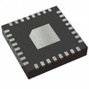
Image may be representation.
See specifications for product details.
EXPRESS OPTION
Payment method

ADS6144IRHBT - Texas Instruments

Manufacturer Part Number
ADS6144IRHBT
Manufacturer
Texas Instruments
Allelco Part Number
98D-ADS6144IRHBT
Warranty
1 Year Allelco Warranty - Find out more
Stock Status:
45,744 pcs available, New & Original
Parts Description
IC ADC 14BIT PIPELINED 32VQFN
Package
32-VQFN (5x5)
Data sheet
ADS6144IRHBT.pdf
RoHs Status
ROHS3 Compliant
Our certification
In stock: 45744
  • Unit Price: $53.855
  • Subtotal: $0.00

Want a better price?
Add to Cart and Submit RFQ now, we'll contact you immediately.

Quantity Unit Price Ext. Price
1+ $53.855 $53.86
The above prices does not include taxes and freight rates, which will be calculated on the order pages.

Specifications

ADS6144IRHBT Tech Specifications
Texas Instruments - ADS6144IRHBT technical specifications, attributes, parameters and parts with similar specifications to Texas Instruments - ADS6144IRHBT

Product Attribute Attribute Value
Manufacturer Texas Instruments
Voltage - Supply, Digital 1.65V ~ 3.6V
Voltage - Supply, Analog 3V ~ 3.6V
Supplier Device Package 32-VQFN (5x5)
Series -
Sampling Rate (Per Second) 105M
Reference Type External, Internal
Ratio - S/H:ADC 1:1
Package / Case 32-VFQFN Exposed Pad
Package Tape & Reel (TR)
Operating Temperature -40°C ~ 85°C
Product Attribute Attribute Value
Number of Inputs 1
Number of Bits 14
Number of A/D Converters 1
Mounting Type Surface Mount
Input Type Differential
Features -
Data Interface LVDS - Parallel, Parallel
Configuration S/H-ADC
Base Product Number ADS6144
Architecture Pipelined

Environmental & Export Classifications

ATTRIBUTE DESCRIPTION
RoHs Status ROHS3 Compliant
Moisture Sensitivity Level (MSL) 3 (168 Hours)
REACH Status REACH Unaffected
ECCN 3A991C3
HTSUS 8542.39.0001

Frequently Asked Questions(FAQ)

How does the ADS6144IRHBT's sampling rate of 105 MSPS compare to other pipelined ADCs in its resolution class, and what design trade-offs might this imply for high-speed signal acquisition systems?
The ADS6144IRHBT achieves a sampling rate of 105 million samples per second (MSPS), which places it among the higher-performance 14-bit pipelined analog-to-digital converters (ADCs). In comparison, many 14-bit pipelined devices typically range from 65 MSPS to 80 MSPS, with some reaching up to 125 MSPS. This level of performance supports bandwidths well beyond 30 MHz when accounting for Nyquist considerations, making it suitable for applications such as software-defined radio (SDR) front-ends and multi-channel radar systems. However, higher sampling rates often come with increased power consumption and more stringent requirements on anti-aliasing filter design. For the ADS6144IRHBT specifically, operating at 105 MSPS within a 3 V analog supply implies careful attention to noise margins and timing synchronization in high-speed parallel LVDS interfaces.
What are the key differences between using an internal versus external reference with the ADS6144IRHBT, and how do these choices affect system-level accuracy in precision measurement applications?
The ADS6144IRHBT supports both internal and external reference options, offering flexibility depending on application needs. An internal reference provides convenience and reduced component count but typically exhibits lower initial accuracy—often around ±1%—and limited temperature drift characteristics. In contrast, an external precision voltage reference can deliver superior stability and lower noise, which is critical for maintaining absolute accuracy over time and temperature. For high-resolution applications requiring long-term calibration stability, such as industrial process control or medical instrumentation, selecting an external reference with low drift (<10 ppm/°C) significantly improves system performance. The ADS6144IRHBT’s differential input architecture further benefits from clean reference sources by minimizing common-mode errors introduced during signal conditioning stages.
Can the ADS6144IRHBT be used effectively in single-ended input configurations, and what modifications are necessary to maintain optimal dynamic performance?
While the ADS6144IRHBT is designed primarily for differential inputs, it can accept single-ended signals by driving one input while grounding the opposite input through a matched impedance path. However, this configuration introduces several challenges: reduced common-mode rejection ratio (CMRR), increased susceptibility to ground noise, and degraded linearity due to imbalance. To mitigate these effects, proper layout symmetry, guard rings, and low-inductance return paths are essential. Additionally, a high-quality differential driver amplifier should precede the ADC to restore signal integrity. In practice, many designs opt for a fully differential source to preserve the full dynamic range and spurious-free dynamic range (SFDR) expected from the ADS6144IRHBT’s architecture—especially important given its 14-bit resolution and 105 MSPS throughput.
How does the ADS6144IRHBT handle clock jitter sensitivity at its maximum sampling rate, and what impact does this have on SNR performance in real-world RF sampling scenarios?
At 105 MSPS, the ADS6144IRHBT exhibits increasing sensitivity to input clock jitter, which directly affects signal-to-noise ratio (SNR). Theoretical calculations show that even sub-picosecond RMS jitter can degrade SNR by several decibels. For example, 1 ps of RMS jitter at 100 MHz input results in approximately –70 dBc of integrated phase noise contribution, pushing total SNR below 70 dB in ideal conditions—well below the theoretical maximum for a 14-bit ADC (~86 dB). Therefore, achieving best-in-class performance requires a low-jitter clock source, such as a disciplined oscillator or VCXO with <0.5 ps RMS jitter. System designers must also consider PCB trace routing and termination to minimize clock feedthrough into analog inputs, particularly when interfacing with parallel LVDS output stages.
What is the typical power consumption profile of the ADS6144IRHBT across different operational modes, and how can engineers optimize energy efficiency without sacrificing speed or resolution?
The ADS6144IRHBT consumes approximately 1.2 W under full-speed operation with both analog and digital supplies active—3.3 V analog and 3.3 V digital. This includes power drawn by the internal reference, sample-and-hold circuitry, and LVDS output drivers. Power scales non-linearly with sampling rate; reducing throughput to 50 MSPS may lower consumption by only ~30%, indicating significant fixed overhead. To improve efficiency, users can disable unused features such as the internal reference if an external source is employed, reduce the number of active LVDS lanes, or employ burst-mode sampling where feasible. Additionally, dynamic voltage scaling (within specified ranges) offers limited benefit but requires careful validation of aperture uncertainty and settling times across process-voltage-temperature (PVT) corners.
How does the ADS6144IRHBT’s package thermal performance affect long-term reliability in compact, high-throughput embedded designs?
The 32-VQFN (5x5 mm) package features an exposed thermal pad that enhances heat dissipation compared to standard QFN packages, yet at sustained 105 MSPS operation, junction temperatures can rise above 70°C even with modest airflow. Without adequate heatsinking or copper pours beneath the thermal pad, thermal resistance may exceed 30°C/W, leading to potential reliability concerns over time, especially near the upper end of the –40°C to +85°C operating range. Engineers should conduct worst-case thermal simulations using tools like ANSYS Icepak or similar, ensuring continuous duty cycles remain within safe limits. Implementing proper via stitching under the thermal pad and connecting it to multiple inner-layer ground planes improves heat spreading, thereby extending MTBF in mission-critical applications like defense electronics or telecom infrastructure.
In what ways does the parallel LVDS interface of the ADS6144IRHBT simplify FPGA integration compared to serial LVDS or SPI-based alternatives?
The ADS6144IRHBT outputs data via a wide parallel LVDS bus (typically 14 bits plus status flags), enabling direct mapping into FPGA input buffers without complex deserialization logic. This contrasts sharply with serial LVDS implementations that require dedicated serializer/deserializer (SerDes) cores and consume significant FPGA resources. With parallel LVDS, FPGA designers gain deterministic timing closure, easier debugging via oscilloscope probing, and simplified alignment between sample index and data word boundaries. However, the trade-off involves increased pin count and tighter skew tolerances—sub-100 ps channel matching becomes critical to prevent bit errors during capture. For high-speed backplane designs, AC-coupled LVDS links with controlled impedance traces (e.g., 100 Ω differential) are recommended to maintain signal integrity across board edges.
What precautions should be taken when cascading multiple ADS6144IRHBT devices for extended resolution or multi-channel systems?
Cascading ADCs like the ADS6144IRHBT is generally discouraged due to inherent limitations in mismatch between units and difficulty in synchronizing internal pipeline stages. Instead, most multi-channel systems use independent ADCs with shared clocks and references, leveraging FPGA-based digital correction algorithms for calibration. If synchronization is required (e.g., in phased-array radar), precise clock distribution networks with zero-skew fanout buffers are essential. Additionally, each device must operate from a tightly matched reference source to avoid offset errors accumulating across channels. Given the complexity, TI recommends evaluating alternative architectures such as interleaved ADCs or specialized multi-chip modules (MCMs) tailored for coherent sampling before committing to a cascade approach with the ADS6144IRHBT.
How does the moisture sensitivity level (MSL) rating of MSL 3 for the ADS6144IRHBT influence handling procedures during reflow soldering in mass production environments?
As an MSL 3 component (requiring storage at <60% RH and max floor life of 168 hours after exposure to ambient conditions), the ADS6144IRHBT demands strict adherence to JEDEC J-STD-033 guidelines. Once removed from moisture-barrier bags, the device must be baked prior to reflow if stored beyond 168 hours, typically at 125°C for 24 hours to drive off absorbed moisture. Failure to follow this protocol risks popcorning during reflow, which can cause internal delamination or bond wire lift-off, particularly problematic for fine-pitch QFN packages like the 32-VQFN. Production lines should implement real-time tracking of bag opening dates and integrate inline moisture sensors in dry cabinets to ensure compliance throughout assembly cycles.
What role does the S/H-to-ADC ratio play in the ADS6144IRHBT’s architecture, and why is a 1:1 ratio beneficial for transient response in bursty signal environments?
The 1:1 sample-and-hold (S/H) to ADC ratio means that each conversion cycle begins immediately after the previous one ends, eliminating idle periods between conversions. This synchronous operation ensures consistent aperture delay across all samples, crucial for maintaining phase accuracy in wideband signals. In burst-mode applications—such as pulsed radar or LiDAR—this predictability allows precise triggering of subsequent processing blocks without introducing variable latency. Furthermore, the absence of dead time between conversions maximizes effective throughput, enabling true real-time capture of transient events lasting just a few nanoseconds. For the ADS6144IRHBT, this design choice complements its pipelined architecture by ensuring no pipeline bubbles disrupt the data stream during sustained high-speed operation.
How does the ADS6144IRHBT perform in terms of integral nonlinearity (INL) and differential nonlinearity (DNL) at 105 MSPS, and what design implications arise from its published specifications?
According to TI’s characterization data, the ADS6144IRHBT exhibits typical INL of ±1.5 LSB and DNL better than ±0.8 LSB across the full temperature range. These values indicate good linearity suitable for imaging and instrumentation applications, though not sufficient for highest-precision metrology without calibration. Notably, DNL remains monotonic, preventing missing codes—a critical requirement for unipolar signal chains. However, INL variations may necessitate digital background calibration in systems demanding sub-LSB accuracy over extended periods. Layout parasitics, especially near analog inputs, can exacerbate these nonlinearities, so careful PCB stackup and guard shielding are advised to preserve linearity claims in deployed hardware.
Can the ADS6144IRHBT operate reliably with a 1.8 V digital supply while running at full speed, and what considerations apply for mixed-voltage interface compatibility?
Yes, the ADS6144IRHBT supports digital supplies down to 1.65 V, making 1.8 V operation fully compliant. This feature facilitates coexistence with modern FPGAs and processors operating at lower voltages, reducing overall system power. However, interfacing between 1.8 V CMOS logic and the ADC’s LVDS outputs requires level-shifting considerations since LVDS inherently uses 3.3 V swing. Direct connection is unsafe; instead, use LVDS receivers rated for 1.8 V operation or implement resistive termination networks that clamp voltage excursions. Additionally, ensure that setup and hold times relative to the 1.8 V core clock meet timing constraints, as reduced supply lowers transistor drive strength and increases propagation delays slightly.
What are the recommended decoupling strategies for stabilizing the ADS6144IRHBT’s dual-supply rails in noisy industrial environments?
Stable analog and digital supplies are critical for achieving advertised performance. Each supply pin should be bypassed with a 1 µF ceramic capacitor placed within 1 mm of the pin, supplemented by a 0.1 µF capacitor closer still. Ferrite beads may be added selectively on the analog rail if switching regulators feed the system, but care must be taken not to attenuate high-frequency noise components essential for ADC performance. Ground planes must remain unbroken beneath the ADC footprint, and split planes avoided unless isolated with star-point connections. For radiated interference immunity, conformal coating or shielded enclosures should be evaluated based on EMC test results in final systems using the ADS6144IRHBT.
How does the ADS6144IRHBT’s operating temperature range affect performance in automotive or outdoor sensing applications, and are derating recommendations necessary?
Operating from –40°C to +85°C covers most industrial and commercial use cases but excludes extreme environments like automotive hot soak (up to 125°C). Within the specified range, parametric drift is managed through internal compensation, though users should verify key metrics—especially SFDR and THD—at temperature extremes via characterization. Derating is not formally mandated by TI, but best practices suggest limiting continuous operation above 70°C to reduce aging effects on internal passives and interconnects. Thermal cycling fatigue remains a latent concern for solder joints in fine-pitch QFN packages, so accelerated life testing per AEC-Q100 (if qualified) is advisable for safety-critical deployments.
What documentation and development tools are available to accelerate evaluation and bring-up of the ADS6144IRHBT in custom hardware platforms?
Texas Instruments provides the ADS6144EVM evaluation module featuring breakout boards, reference layouts, and GUI-based control software compatible with Windows/Linux. Additionally, SPICE models, IBIS simulations, and HDL code examples (VHDL/Verilog) are accessible via TI’s Resource Explorer. Designers can leverage the TIDesigner toolchain for signal chain optimization, including driver selection, anti-alias filtering, and power sequencing analysis. Reference schematics for FPGA interfaces (e.g., Xilinx Artix-7 or Intel Cyclone V) are included, along with layout guidelines emphasizing 4-layer stackups with solid ground planes and controlled impedance routing for LVDS signals. These resources collectively reduce time-to-market for systems integrating the ADS6144IRHBT.
How does the ADS6144IRHBT compare to the ADS62Pxxx family in terms of resolution-speed trade-offs, and which would be preferable for broadband spectrum monitoring?
While both families target high-speed acquisition, the ADS6144IRHBT offers 14-bit resolution at 105 MSPS, whereas the ADS62Pxxx series provides 12-bit at up to 125 MSPS. The latter trades resolution for higher throughput and lower power, making it ideal for wideband RF digitization where dynamic range requirements are less stringent. For spectrum monitoring requiring moderate resolution with broad coverage (e.g., detecting weak signals across large bandwidths), the ADS62Pxxx may suffice. However, if fine amplitude discrimination or harmonic analysis is needed, the ADS6144IRHBT’s extra two bits provide meaningful improvement in SFDR and effective number of bits (ENOB), albeit at higher cost and power. Selection ultimately depends on whether spectral purity or acquisition speed dominates system priorities.
Are there known limitations or errata associated with the ADS6144IRHBT that could impact system robustness in production deployments?
As of latest datasheet revision (SPRSE24), TI lists no open errata, but several application notes highlight design sensitivities: first, simultaneous switching noise (SSN) on digital outputs can couple into analog inputs if return paths are poorly managed; second, improper initialization sequences may leave the ADC in undefined states—always reset pipelines before first conversion; third, LVDS receiver thresholds vary with temperature, necessitating margining in FPGA firmware. Additionally, note that the internal reference turns off automatically during shutdown, so re-enabling it requires warm-up time (~10 ms). While not defects per se, these behaviors must be accounted for in robust state machines managing the ADS6144IRHBT in field-deployed equipment.

Parts with Similar Specifications

The three parts on the right have similar specifications to Texas Instruments ADS6144IRHBT

Product Attribute ADS6144IRHB25 ADS6142IRHBTG4 ADS6144IRHBR ADS6145IRHBT
Part Number ADS6144IRHB25 ADS6142IRHBTG4 ADS6144IRHBR ADS6145IRHBT
Manufacturer Texas Instruments Luminary Micro / Texas Instruments Texas Instruments Texas Instruments
Number of Inputs - - - 2
Supplier Device Package - 196-NFBGA (12x12) 16-PDIP 64-VQFN (9x9)
Sampling Rate (Per Second) - - - 65M
Voltage - Supply, Digital - 1.14V ~ 1.26V 11.4V ~ 16.5V 1.65V ~ 3.6V
Data Interface - LVDS - Parallel I²C LVDS - Parallel, Parallel
Configuration - - - S/H-ADC
Package - Tape & Reel (TR) Tube Tape & Reel (TR)
Input Type - - - Differential
Ratio - S/H:ADC - - - 1:1
Number of A/D Converters - - - 2
Architecture - Current Source R-2R Pipelined
Reference Type - External, Internal External External, Internal
Mounting Type - Surface Mount Through Hole Surface Mount
Voltage - Supply, Analog - 3.14V ~ 3.46V 11.4V ~ 16.5V 3V ~ 3.6V
Features - - - Simultaneous Sampling
Series - - - -
Number of Bits - 16 8 14
Operating Temperature - -40°C ~ 85°C 0°C ~ 70°C -40°C ~ 85°C
Package / Case - 196-LFBGA 16-DIP (0.300', 7.62mm) 64-VFQFN Exposed Pad
Base Product Number - DAC34H84 MAX500 ADS62P42

ADS6144IRHBT Datasheet PDF

Download ADS6144IRHBT pdf datasheets and Texas Instruments documentation for ADS6144IRHBT - Texas Instruments.

PCN Design/Specification
Copper Wire Base Metal 19/Jun/2014.pdf Copper Wire Revision B 16/Dec/2014.pdf
HTML Datasheet
ADS6142-6145.pdf ADS6142-45.pdf

Customer Reviews

Evaluation: 10 Articles

  • Dani***alkerTech
    Jun 1, 2026

    Product works, but setup took more effort than expected. Once configured the MCU ran reliably, although documentation support felt older compared with newer platforms. Fine for maintenance projects.

  • Yuki***aka88
    May 26, 2026

    信号通信プロジェクトでこのRS-485トランシーバーを使用しました。設置は簡単で、長距離ケーブルでも通信は安定していました。消費電力も、以前使用していたものより低くなっています。

  • Stev***aker
    May 20, 2026

    Solid diode for power rectification. Works well in switching circuits.

  • Bran***Lewis
    May 11, 2026

    Compact FPGA with good performance. Suitable for basic signal processing tasks.

  • Oliv***arris
    May 7, 2026

    Reliable I/O expander. Works well in embedded control applications.

  • Jess***Jones
    Apr 17, 2026

    It offers good value for the price, and the specifications match the description. I’ve been using it for two days with no issues, and I’ll definitely buy it again if I need it in the future.

  • Mich***Smith
    Apr 17, 2026

    Shipping was on time, the component pins are neatly aligned, and I tested 10 of them with a multimeter—all readings were within the specified range. Highly recommended.

  • Aman***arris
    Apr 3, 2026

    It was great—the entire process, from placing the order to receiving the package, went very smoothly. The components were consistent, the price was fair, and I had a very pleasant shopping experience.

  • Mike***nch
    Apr 3, 2026

    Better than expected! The resistance and capacitance readings were spot-on, and it passed the test on the first try. The service was reliable, and the packaging was thoughtful—I highly recommend it.

  • Daic***K.
    Mar 23, 2026

    Very good. No issue after long time testing.

Write a Review

Your Email address will not be published.

Shipment

Delivery Time

In-stock items can be shipped within 24 hours. Some parts will be arranged for delivery within 1-2 days from the date all items arrive at our warehouse. And Allelco ships order once a day at about 17:00, except Sunday. Once the goods are shipped, the estimated delivery time depends on the shipping methods and Delivery destination. The table below shows are the logistic time for some common countries.

Delivery Cost

  1. Use your express account for shipment if you have one.
  2. Use our account for the shipment. Refer to the table below for the approximate charges.
(Different time frame / countries / package size has different price.)

Delivery Method

  1. Global Common Shipment by DHL / UPS / FedEx / TNT / EMS / SF we support.
  2. Others more shipping ways, please get in touch with your customer manager.

Common Countries Logistic Time Reference
Region Country Logistic Time(Day)
America United States 5
Brazil 7
Europe Germany 5
United Kingdom 4
Italy 5
Oceania Australia 6
New Zealand 5
Asia India 4
Japan 4
Middle East Israel 6
DHL & FedEx Shipment Charges Reference
Shipment charges(KG) Reference DHL(USD$)
0.00kg-1.00kg USD$30.00 - USD$60.00
1.00kg-2.00kg USD$40.00 - USD$80.00
2.00kg-3.00kg USD$50.00 - USD$100.00
Note:
The above table is for reference only. There may have some data bias for the uncontrollable factors.
Contact us if you have any questions.
  • QC (Quality Warranty)
  • Payment Support
  • Packaging
  • Certifications & Memberships

QC (Quality Warranty)

Allelco is committed to exceeding customer expectations through customer service excellence, order accuracy, and on-time delivery.
This is achieved through our commitment to the continual improvement of our processes, services, and products.


Strict quality inspection builds a solid foundation for electronic component quality.
  1. Visual inspection
  2. Performance testing and reliability verification
  3. Standardized full-process testing
  4. Precise control of every parameter
We eliminate defective components and ensure the stable operation of electronic devices through professional quality standards.

Payment Support

The payment method can be chosen from the methods shown below: Wire Transfer (T/T, Bank Transfer), Western Union, Credit card, PayPal.
  • HKBea
  • Paypal
  • MasterCard
  • Western-Union
  • VISA
Stable Delivery, Sincere Partnership — Your Faithful Supply Chain Partner
  • Efficient Supply Management
  • Cost-Saving Procurement
  • Fast Sourcing & Delivery
Contact us if you have any questions.

Packaging

Electrostatic Discharge Protection and Handling

All electrostatic-sensitive components are handled in accordance with electrostatic discharge control procedures. The products are hermetically sealed in anti-static safe packaging to prevent electrostatic damage. Appropriate labeling is also applied for identification and traceability. This ensures product integrity during storage, handling and transportation.


ESD

Certifications & Memberships

Third-party certified, strict quality control. Our certification
  • ISO 9001: 2015
  • ISO 13485: 2016
  • ISO 14001: 2015
  • ISO 28000: 2007
  • ISO 45001: 2018
  • GB/T 27922-2011
  • SMTA
  • IPC
  • ESD
  • PSMA
ADS6144IRHBT Image

ADS6144IRHBT

Texas Instruments
98D-ADS6144IRHBT

Want a better price? Add to Cart and Submit RFQ now, we'll contact you immediately.

0 RFQ
Shopping cart (0 Items)
It is empty.
Compare List (0 Items)
It is empty.
Feedback

Your feedback matters! At Allelco, we value the user experience and strive to improve it constantly.
Please share your comments with us via our feedback form, and we'll respond promptly.
Thank you for choosing Allelco.

Subject
E-mail
Comments
Captcha
Drag or click to upload file
Upload File
types: .xls, .xlsx, .doc, .docx, .jpg, .png and .pdf.
Max file size: 10MB