 ADS6144IRHB25Texas InstrumentsIC ADC 14BIT PIPELINED 32VQFN
 ADS61B23EVMTexas InstrumentsEVAL MODULE FOR ADS61B23
 ADS6145IRHBT REELTexas InstrumentsADS6145IRHBT REEL
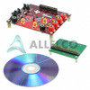 ADS6145EVMTexas InstrumentsEVAL MOUDLE FOR ADS6145
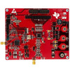 ADS6149EVMTexas InstrumentsEVALUATION MODULE FOR ADS6149
 ADS6149IRGZTexas Instruments
- Dani***alkerTech
- Jun 1, 2026
HomeProductsIntegrated Circuits (ICs)Data Acquisition - Analog to Digital Converters (ADC)ADS6148IRGZ25


Image may be representation.
See specifications for product details.
See specifications for product details.
- EXPRESS OPTION
- Payment method
ADS6148IRGZ25 - Texas Instruments
- Manufacturer Part Number
- ADS6148IRGZ25
- Manufacturer
- Texas Instruments
- Allelco Part Number
- 98D-ADS6148IRGZ25
- Warranty
- 1 Year Allelco Warranty - Find out more
- Stock Status:
- 11,809 pcs available, New & Original
- Parts Description
- IC ADC 14BIT PIPELINED 48VQFN
- Package
- 48-VQFN (7x7)
- Data sheet
-
ADS6148IRGZ25.pdf
HTML Datasheet
ADS6128,29,48,49.pdf
- RoHs Status
- ROHS3 Compliant
- Our certification
- In stock: 11809


