

ADS6148IRGZR (1)
Manufacturer Part Number
ADS6148IRGZR
Manufacturer
Texas Instruments
Introduction
ADS6148IRGZR is a high-speed, 14-bit Analog to Digital Converter (ADC) featuring a maximum sampling rate of 210M samples per second with differential input type, primarily designed for advanced digital data acquisition.
Product Features and Performance
14-bit resolution
Maximum sampling rate of 210M samples per second
Single differential input
LVDS and parallel data interfaces
Pipelined architecture
Support for both external and internal reference voltages
Operates with analog supply voltage from 3V to 3.6V and digital supply voltage from 1.7V to 1.9V
Adaptable with surface mount technology
Product Advantages
High-speed data sampling capacity enhances real-time performance
Dual-mode reference voltage increases flexibility in varying conditions
Compact 48-VFQFN Exposed Pad package facilitates efficient usage of PCB space
Key Technical Parameters
Number of Bits: 14
Sampling Rate (Per Second): 210M
Input Type: Differential
Voltage - Supply, Analog: 3V ~ 3.6V
Voltage - Supply, Digital: 1.7V ~ 1.9V
Operating Temperature: -40°C ~ 85°C
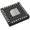
Package / Case: 48-VFQFN Exposed Pad
Quality and Safety Features
Operates within a broad temperature range of -40°C to 85°C ensuring stability under extreme conditions
Quality ensured by Texas Instruments' rigorous testing and validation processes
Compatibility
Compatible with devices requiring LVDS or parallel data input interfaces
Surface mount compatibility suitable for modern PCB technology
Application Areas
Telecommunications
Data acquisition systems
Medical imaging equipment
Industrial automation and control systems
Product Lifecycle
Currently in active production status
Manufacturer ensures ongoing support and availability
Several Key Reasons to Choose This Product
Extremely fast sampling rate enables the capture of quick signal variations
High resolution facilitates precise data conversion from analog to digital
Robust operating temperature range ensures reliability in harsh environments
Compatibility with modern mounting technologies reduces hardware design complexities
Trusted manufacturer with a global reputation in semiconductor solutions
 ADS61B23IRHB25Texas InstrumentsIC ADC 12BIT PIPELINED 32VQFN
 ADS6149EVMTexas InstrumentsEVALUATION MODULE FOR ADS6149
 ADS61B23EVMTexas InstrumentsEVAL MODULE FOR ADS61B23
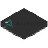 ADS6145IRHBT REELTexas InstrumentsADS6145IRHBT REEL
 ADS6145EVMTexas InstrumentsEVAL MOUDLE FOR ADS6145
 ADS6149IRGZTexas Instruments


