View All

Please refer to the English Version as our Official Version.Return

Europe
France(Français) Germany(Deutsch) Italy(Italia) Russian(русский) Poland(polski) Czech(Čeština) Luxembourg(Lëtzebuergesch) Netherlands(Nederland) Iceland(íslenska) Hungarian(Magyarország) Spain(español) Portugal(Português) Turkey(Türk dili) Bulgaria(Български език) Ukraine(Україна) Greece(Ελλάδα) Israel(עִבְרִית) Sweden(Svenska) Finland(Svenska) Finland(Suomi) Romania(românesc) Moldova(românesc) Slovakia(Slovenská) Denmark(Dansk) Slovenia(Slovenija) Slovenia(Hrvatska) Croatia(Hrvatska) Serbia(Hrvatska) Montenegro(Hrvatska) Bosnia and Herzegovina(Hrvatska) Lithuania(lietuvių) Spain(Português) Switzerland(Deutsch) United Kingdom(English)
Asia/Pacific
Japan(日本語) Korea(한국의) Thailand(ภาษาไทย) Malaysia(Melayu) Singapore(Melayu) Vietnam(Tiếng Việt) Philippines(Pilipino)
Africa, India and Middle East
United Arab Emirates(العربية) Iran(فارسی) Tajikistan(فارسی) India(हिंदी) Madagascar(malaɡasʲ)
South America / Oceania
New Zealand(Maori) Brazil(Português) Angola(Português) Mozambique(Português)
North America
United States(English) Canada(English) Haiti(Ayiti) Mexico(español)
HomeProductsIntegrated Circuits (ICs)Linear - Amplifiers - Instrumentation, OP Amps, Buffer AmpsINA1620RTWT
INA1620RTWT Image
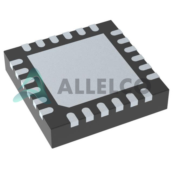
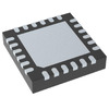
Image may be representation.
See specifications for product details.
EXPRESS OPTION
Payment method

INA1620RTWT - Texas Instruments

Manufacturer Part Number
INA1620RTWT
Manufacturer
Texas Instruments
Allelco Part Number
98D-INA1620RTWT
Warranty
1 Year Allelco Warranty - Find out more
Stock Status:
48,900 pcs available, New & Original
Parts Description
IC AUDIO 2 CIRCUIT 24WQFN
Package
24-WQFN (4x4)
Data sheet
INA1620RTWT.pdf

HTML Datasheet

INA1620.pdf
RoHs Status
ROHS3 Compliant
Our certification
In stock: 48900
  • Unit Price: $8.253
  • Subtotal: $0.00

Want a better price?
Add to Cart and Submit RFQ now, we'll contact you immediately.

Quantity Unit Price Ext. Price
1+ $8.253 $8.25
250+ $3.194 $798.50
500+ $3.082 $1,541.00
1000+ $3.026 $3,026.00
The above prices does not include taxes and freight rates, which will be calculated on the order pages.

Specifications

INA1620RTWT Tech Specifications
Texas Instruments - INA1620RTWT technical specifications, attributes, parameters and parts with similar specifications to Texas Instruments - INA1620RTWT

Product Attribute Attribute Value
Manufacturer Texas Instruments
Voltage - Supply Span (Min) 4 V
Voltage - Supply Span (Max) 36 V
Voltage - Input Offset 100 µV
Supplier Device Package 24-WQFN (4x4)
Slew Rate 10V/µs
Series -
Package / Case 24-WFQFN Exposed Pad
Package Tape & Reel (TR)
Output Type -
Product Attribute Attribute Value
Operating Temperature -40°C ~ 125°C
Number of Circuits 2
Mounting Type Surface Mount
Gain Bandwidth Product 32 MHz
Current - Supply 2.6mA (x2 Channels)
Current - Output / Channel 145 mA
Current - Input Bias 1.2 µA
Base Product Number INA1620
Amplifier Type Audio

Environmental & Export Classifications

ATTRIBUTE DESCRIPTION
RoHs Status ROHS3 Compliant
Moisture Sensitivity Level (MSL) 2 (1 Year)
REACH Status REACH Unaffected
ECCN EAR99

Frequently Asked Questions(FAQ)

How does the INA1620RTWT compare to other dual-channel audio amplifiers in terms of power supply range and efficiency under typical 16V operation?
The INA1620RTWT operates across a wide supply voltage span from 4 V to 36 V, making it suitable for both low-voltage battery-powered applications and high-voltage industrial setups. At 16 V, each channel draws approximately 2.6 mA quiescent current, which translates to an effective quiescent power consumption of around 83 mW per channel. This level of idle power is competitive with similar-class dual amplifiers such as the TPA3116 or LM4602, though those often require higher supply rails or exhibit greater quiescent draw at lower voltages. The INA1620’s combination of rail-to-rail input/output capability and moderate quiescent current allows efficient operation in Class AB configurations without significant crossover distortion, especially when driving loads above 4 Ω.
What are the thermal implications of using the INA1620RTWT in a compact 24-WQFN package when delivering 1 W into an 8 Ω load?
Delivering 1 W into an 8 Ω load requires approximately 283 mA RMS output current per channel, assuming unity gain. With a typical supply of ±15 V (30 V span), total power dissipation per channel can reach roughly 0.85 W due to conduction losses. In the 24-WQFN (4x4) package with exposed pad, this results in junction-to-ambient thermal resistance of about 45°C/W, leading to a temperature rise of nearly 39°C above ambient. At 25°C room temperature, the junction could reach 64°C, well within the -40°C to 125°C operating range. However, continuous full-power operation in tightly spaced designs may require careful PCB copper layout and airflow assessment to avoid thermal throttling or long-term reliability concerns.
Can the INA1620RTWT be safely used in automotive audio systems with frequent start-stop cycles and cold cranking transients?
Yes, the INA1620RTWT is rated for operation from -40°C to 125°C and supports supply voltages up to 36 V, which accommodates typical automotive battery conditions including cold crank events down to 3 V and transient spikes up to 40 V (within absolute maximum ratings). Its input offset voltage of 100 µV ensures minimal DC error during low-voltage operation, while the 1.2 µA input bias current remains negligible even with high-impedance source stages. These characteristics make it suitable for automotive head units, infotainment amplifiers, and subwoofer drivers where power stability fluctuates significantly. Proper decoupling near the IC and adherence to EMC layout practices further enhance robustness in harsh environments.
How does the slew rate and bandwidth of the INA1620RTWT impact its performance when driving capacitive loads or high-frequency PWM signals?
With a slew rate of 10 V/µs and a gain-bandwidth product of 32 MHz, the INA1620RTWT can handle audio frequencies up to several hundred kHz without phase degradation. However, driving capacitive loads—such as long speaker cables or unterminated outputs—can cause instability if compensation capacitors are not properly managed. The internal frequency compensation is designed for resistive loads, so external series resistors (typically 10–100 Ω) are recommended when capacitive loading exceeds 10 nF. In PWM-to-analog filtering applications, the 32 MHz GBW ensures clean reconstruction of high-frequency modulated signals without slew-induced distortion, provided the feedback network maintains sufficient phase margin.
When selecting between the INA1620RTWT and discrete op-amp solutions for audio signal conditioning, what design trade-offs should be considered?
The INA1620RTWT integrates two precision audio amplifiers in a single chip, offering matched channels with low input offset (100 µV) and high PSRR—critical for maintaining signal integrity in noisy power environments. Compared to discrete op-amps, it reduces board space by over 60%, simplifies layout, and minimizes crosstalk through shared substrate design. However, discrete solutions offer greater flexibility in gain setting, slew customization, and thermal isolation. For stereo line-level preamplification or impedance buffering, the INA1620 provides superior integration and consistency; for high-current push-pull stages requiring custom biasing, discrete BJTs or MOSFETs may yield better efficiency. The choice hinges on system complexity versus performance predictability.
What precautions should be taken when mounting the INA1620RTWT on a PCB to ensure optimal thermal and electrical performance?
The INA1620RTWT uses a 24-WQFN package with an exposed thermal pad that must be soldered directly to a solid ground plane on the PCB to maximize heat dissipation and electrical connectivity. Minimum recommended copper area is 1.2 cm² with multiple vias (at least four 0.3 mm diameter vias) connecting the pad to inner or bottom-layer ground planes. Avoid placing high-current traces adjacent to sensitive analog inputs, and maintain guard rings around input pins to reduce coupling from switching regulators or digital noise. Use low-ESR ceramic bypass capacitors (10 µF bulk + 0.1 µF MLCC) placed within 2 mm of the V+ and GND pins. This layout minimizes loop inductance and ensures stable operation under dynamic load conditions.
How does the Moisture Sensitivity Level (MSL) of 1 for the INA1620RTWT affect handling and storage requirements during manufacturing?
With an MSL rating of 1, the INA1620RTWT is not susceptible to moisture absorption and can remain unprotected indefinitely before assembly. This simplifies inventory management and eliminates the need for baking prior to reflow soldering, unlike components rated MSL 2 or higher. However, standard anti-static precautions still apply due to its CMOS construction. Storage should occur in ESD-protected containers at ambient conditions below 60% relative humidity to prevent condensation during environmental testing or field deployment in humid climates. No special handling procedures are mandated beyond general semiconductor best practices.
Is the INA1620RTWT suitable for use in medical audio monitoring equipment requiring low noise and high CMRR?
While the INA1620RTWT delivers low input offset and modest noise performance typical of audio-grade amplifiers, its noise density (~40 nV/√Hz) may exceed requirements for sensitive biomedical signal acquisition where ECG or EEG signals are amplified directly. Medical-grade instrumentation usually demands specialized low-noise, low-drift amplifiers like the INA128 or AD8421, which offer lower 1/f noise corner and higher CMRR (>100 dB). That said, the INA1620RTWT can serve in auxiliary audio paths—such as patient alert tones or voice prompts—where primary signal fidelity is secondary. Its rail-to-rail inputs and wide supply range add value in portable medical devices powered by batteries, but not in core sensing stages.
What is the impact of the 2.6 mA supply current per channel on battery life in portable audio applications using the INA1620RTWT?
At 2.6 mA quiescent current per channel, the INA1620RTWT consumes about 5.2 mA total when both channels are active. Assuming a 3.7 V lithium-ion battery and 85% amplifier efficiency, this corresponds to approximately 19 mW idle power. Over eight hours of playback, this adds only ~55 mAh to the load, representing less than 5% of a typical 1000 mAh battery capacity. When combined with sleep modes or duty-cycled operation, the impact on runtime is minimal. This low quiescent draw compares favorably with many modern audio codecs and DSP chips, making the INA1620RTWT a reasonable choice for battery-powered consumer audio products where standby time matters more than peak efficiency.
How does the operating temperature range influence the selection of the INA1620RTWT for industrial or aerospace audio systems?
The INA1620RTWT’s extended temperature range (-40°C to 125°C) enables deployment in environments where thermal cycling, altitude variations, or prolonged sun exposure occur—common in industrial control panels or aerospace avionics racks. Unlike commercial-grade parts limited to 0°C to 70°C, this device maintains specified parameters at 125°C, ensuring consistent slew rate, bandwidth, and output current capability even under hot-soak conditions. However, long-term reliability at the upper end requires derating output power by 10–15% to account for electromigration effects in the bond wires and metallization. Thermal simulation during design-in is advisable for mission-critical applications where failure modes must be minimized.
Can the INA1620RTWT drive piezoelectric buzzers or ultrasonic transducers effectively?
The INA1620RTWT can drive reactive loads like piezoelectric elements, provided they do not exceed the 145 mA per channel output current limit or introduce excessive capacitive kickback. Piezoelectric buzzers typically present low impedance during activation but generate back-EMF pulses that can stress output stages. Adding a small series resistor (e.g., 10 Ω) limits peak current and protects the IC. Since these devices operate at fixed resonant frequencies (often 2–5 kHz), the 32 MHz GBW and 10 V/µs slew rate ensure clean excitation without distortion. However, for frequencies above 20 kHz (ultrasonic), the open-loop gain rolls off beyond unity, reducing effective drive strength unless closed-loop gain is carefully set to compensate.
What role does the input bias current play in the INA1620RTWT when interfacing with high-impedance sensors or microphone preamps?
The 1.2 µA input bias current of the INA1620RTWT introduces a voltage drop across source resistances, potentially creating DC offset errors in high-Z sensor interfaces. For example, a 10 kΩ source impedance yields a 12 mV offset, which may saturate downstream stages if not accounted for. In microphone applications using electret capsules with built-in FETs, this current is generally negligible due to the capsule’s own biasing. To minimize impact, use low-value source resistors (<1 kΩ) or insert a DC-blocking capacitor followed by a buffer stage. The low bias current nonetheless makes the INA1620RTWT preferable over older bipolar designs with higher Ib, especially in FET-input configurations.
How does the package size of the INA1620RTWT affect routing density in compact wearable audio devices?
The 24-WQFN (4x4 mm) footprint occupies minimal board real estate—approximately 16 mm²—making it ideal for space-constrained wearables like hearables or fitness earbuds. Its thin profile (0.8 mm max) allows placement on both top and bottom layers without height restrictions. However, dense routing demands careful attention to via stitching around the thermal pad and separation of power/ground planes to prevent coupling. Signal traces should avoid crossing split planes or high-speed lines, and differential pairs (if used) must maintain consistent length matching within 0.5 mm. The small size also reduces parasitic capacitance, aiding high-frequency response despite the lack of internal EMI shielding.
What are the limitations of the INA1620RTWT when used in bridged-mono configurations for high-power subwoofer drives?
In bridged mode, the INA1620RTWT can deliver up to 2 × 145 mA = 290 mA peak current into a low-impedance load, but output swing degrades near rails due to internal architecture constraints. Bridging doubles theoretical output power but halves headroom voltage, increasing risk of clipping at high amplitudes. Moreover, the IC lacks built-in dead-time control or shoot-through protection required for safe bridged operation, necessitating external diodes or MOSFETs to isolate outputs and prevent cross-conduction. Additionally, the 10 V/µs slew rate limits how quickly large bass transients can be reproduced, potentially softening attack edges on sharp percussive sounds. For true high-power mono applications, discrete Class D or dedicated bridgeable ICs are more appropriate.
How does RoHS3 compliance of the INA1620RTWT align with global regulatory standards for hazardous substance reduction?
RoHS3 compliance confirms that the INA1620RTWT contains no restricted substances—including lead, mercury, cadmium, hexavalent chromium, PBBs, PBDEs, and phthalates—above threshold levels defined by EU Directive 2011/65/EU. This ensures the component meets export requirements for markets such as Europe, Japan, and California, avoiding customs delays or product recalls. The absence of halogenated flame retardants also improves recyclability and reduces toxicity during disposal. Manufacturers leveraging the INA1620RTWT benefit from streamlined certification processes for end products like medical devices, toys, or IT equipment, where RoHS conformity is mandatory for market access.
What considerations apply when replacing the INA1620RTWT with another dual audio amplifier in an existing design?
Substituting the INA1620RTWT requires verifying compatibility in five key areas: supply range (4–36 V), quiescent current (2.6 mA/ch), output current (145 mA/ch), package footprint (24-WQFN), and thermal performance. Alternatives like the LM4602 or TPA3116D2 may offer higher output power but consume more static current or require larger packages. Pinout differences must be mapped precisely, especially for the exposed pad connection. Additionally, gain bandwidth (32 MHz vs. competitor specs) and slew rate (10 V/µs) affect high-frequency response, which may alter crossover distortion behavior in feedback networks. Simulation with SPICE models is recommended before hardware revision to avoid instability or oscillation issues post-replacement.
How does the ECCN classification of EAR99 affect procurement and shipping logistics for the INA1620RTWT?
With an Export Control Classification Number (ECCN) of EAR99, the INA1620RTWT falls under U.S. Commerce Control List Category EAR99, meaning it is subject to general export regulations but not controlled for national security reasons. This simplifies international procurement—no special licenses are needed for most destinations, and end-use restrictions are minimal. Suppliers can ship directly to customers in countries like China, India, or Brazil without triggering additional compliance checks. However, buyers must still comply with local import duties and ensure final application doesn’t involve military or surveillance uses that could trigger secondary scrutiny. Overall, EAR99 status enhances accessibility for commercial electronics manufacturers worldwide.
Why might the INA1620RTWT be preferred over discrete transistor-based audio stages in modular audio cards?
The INA1620RTWT offers integrated precision, eliminating the need for external biasing networks, heat sinks, or component matching required in discrete designs. Its matched channels ensure identical gain and offset drift over temperature, critical for stereo imaging and balance calibration. Discrete stages demand iterative tuning and occupy more board space, increasing BOM cost and assembly complexity. Furthermore, the INA1620RTWT includes built-in protection against short circuits and thermal overload, reducing design risk in mass-produced modules. For rack-mounted audio I/O cards where reliability, reproducibility, and serviceability are priorities, the monolithic solution provides a robust, compact alternative to hand-assembled transistor pairs.

Parts with Similar Specifications

The three parts on the right have similar specifications to Texas Instruments INA1620RTWT

Product Attribute INA163UA/2K5E4 INA163UA/2K5G4 INA163UA/2K5 INA159AIDGKR
Part Number INA163UA/2K5E4 INA163UA/2K5G4 INA163UA/2K5 INA159AIDGKR
Manufacturer Texas Instruments Texas Instruments Texas Instruments Texas Instruments
Series - - - -
Current - Supply - - - -
Voltage - Supply Span (Min) - - - -
Output Type - Current - Unbuffered Voltage - Buffered -
Operating Temperature - -40°C ~ 85°C 0°C ~ 70°C -40°C ~ 85°C
Current - Output / Channel - - - -
Voltage - Supply Span (Max) - - - -
Number of Circuits - - - -
Amplifier Type - - - -
Base Product Number - DAC34H84 MAX500 ADS62P42
Mounting Type - Surface Mount Through Hole Surface Mount
Package - Tape & Reel (TR) Tube Tape & Reel (TR)
Package / Case - 196-LFBGA 16-DIP (0.300', 7.62mm) 64-VFQFN Exposed Pad
Voltage - Input Offset - - - -
Gain Bandwidth Product - - - -
Current - Input Bias - - - -
Slew Rate - - - -
Supplier Device Package - 196-NFBGA (12x12) 16-PDIP 64-VQFN (9x9)

INA1620RTWT Datasheet PDF

Download INA1620RTWT pdf datasheets and Texas Instruments documentation for INA1620RTWT - Texas Instruments.

HTML Datasheet
INA1620.pdf

Customer Reviews

Evaluation: 10 Articles

  • Emil***rperTech
    Jun 23, 2026

    Works exactly as described. I used it as a USB-to-SPI bridge in a small MCU development project and communication was stable from the first setup.

  • Liam***terTech
    Jun 15, 2026

    Used this CPLD in a logic control project. Programming was straightforward and signal timing matched the design requirements.

  • Nath***rooks
    Jun 11, 2026

    Installed this power component in a converter board. Output remained stable under different load conditions and thermal performance was better than expected.

  • Dani***alkerTech
    Jun 1, 2026

    Product works, but setup took more effort than expected. Once configured the MCU ran reliably, although documentation support felt older compared with newer platforms. Fine for maintenance projects.

  • Yuki***aka88
    May 26, 2026

    信号通信プロジェクトでこのRS-485トランシーバーを使用しました。設置は簡単で、長距離ケーブルでも通信は安定していました。消費電力も、以前使用していたものより低くなっています。

  • Stev***aker
    May 20, 2026

    Solid diode for power rectification. Works well in switching circuits.

  • Bran***Lewis
    May 11, 2026

    Compact FPGA with good performance. Suitable for basic signal processing tasks.

  • Oliv***arris
    May 7, 2026

    Reliable I/O expander. Works well in embedded control applications.

  • Jess***Jones
    Apr 17, 2026

    It offers good value for the price, and the specifications match the description. I’ve been using it for two days with no issues, and I’ll definitely buy it again if I need it in the future.

  • Mich***Smith
    Apr 17, 2026

    Shipping was on time, the component pins are neatly aligned, and I tested 10 of them with a multimeter—all readings were within the specified range. Highly recommended.

Write a Review

Your Email address will not be published.

Shipment

Delivery Time

In-stock items can be shipped within 24 hours. Some parts will be arranged for delivery within 1-2 days from the date all items arrive at our warehouse. And Allelco ships order once a day at about 17:00, except Sunday. Once the goods are shipped, the estimated delivery time depends on the shipping methods and Delivery destination. The table below shows are the logistic time for some common countries.

Delivery Cost

  1. Use your express account for shipment if you have one.
  2. Use our account for the shipment. Refer to the table below for the approximate charges.
(Different time frame / countries / package size has different price.)

Delivery Method

  1. Global Common Shipment by DHL / UPS / FedEx / TNT / EMS / SF we support.
  2. Others more shipping ways, please get in touch with your customer manager.

Common Countries Logistic Time Reference
Region Country Logistic Time(Day)
America United States 5
Brazil 7
Europe Germany 5
United Kingdom 4
Italy 5
Oceania Australia 6
New Zealand 5
Asia India 4
Japan 4
Middle East Israel 6
DHL & FedEx Shipment Charges Reference
Shipment charges(KG) Reference DHL(USD$)
0.00kg-1.00kg USD$30.00 - USD$60.00
1.00kg-2.00kg USD$40.00 - USD$80.00
2.00kg-3.00kg USD$50.00 - USD$100.00
Note:
The above table is for reference only. There may have some data bias for the uncontrollable factors.
Contact us if you have any questions.
  • QC (Quality Warranty)
  • Payment Support
  • Packaging
  • Certifications & Memberships

QC (Quality Warranty)

Allelco is committed to exceeding customer expectations through customer service excellence, order accuracy, and on-time delivery.
This is achieved through our commitment to the continual improvement of our processes, services, and products.


Strict quality inspection builds a solid foundation for electronic component quality.
  1. Visual inspection
  2. Performance testing and reliability verification
  3. Standardized full-process testing
  4. Precise control of every parameter
We eliminate defective components and ensure the stable operation of electronic devices through professional quality standards.

Payment Support

The payment method can be chosen from the methods shown below: Wire Transfer (T/T, Bank Transfer), Western Union, Credit card, PayPal.
  • HKBea
  • Paypal
  • MasterCard
  • Western-Union
  • VISA
Stable Delivery, Sincere Partnership — Your Faithful Supply Chain Partner
  • Efficient Supply Management
  • Cost-Saving Procurement
  • Fast Sourcing & Delivery
Contact us if you have any questions.

Packaging

Electrostatic Discharge Protection and Handling

All electrostatic-sensitive components are handled in accordance with electrostatic discharge control procedures. The products are hermetically sealed in anti-static safe packaging to prevent electrostatic damage. Appropriate labeling is also applied for identification and traceability. This ensures product integrity during storage, handling and transportation.


ESD

Certifications & Memberships

Third-party certified, strict quality control. Our certification
  • ISO 9001: 2015
  • ISO 13485: 2016
  • ISO 14001: 2015
  • ISO 28000: 2007
  • ISO 45001: 2018
  • GB/T 27922-2011
  • SMTA
  • IPC
  • ESD
  • PSMA
INA1620RTWT Image

INA1620RTWT

Texas Instruments
98D-INA1620RTWT

Want a better price? Add to Cart and Submit RFQ now, we'll contact you immediately.

0 RFQ
Shopping cart (0 Items)
It is empty.
Compare List (0 Items)
It is empty.
Feedback

Your feedback matters! At Allelco, we value the user experience and strive to improve it constantly.
Please share your comments with us via our feedback form, and we'll respond promptly.
Thank you for choosing Allelco.

Subject
E-mail
Comments
Captcha
Drag or click to upload file
Upload File
types: .xls, .xlsx, .doc, .docx, .jpg, .png and .pdf.
Max file size: 10MB