 INA159AIDGKRTexas InstrumentsIC OPAMP DIFF 1 CIRCUIT 8VSSOP
 INA157UTexas InstrumentsIC OPAMP DIFF 1 CIRCUIT 8SOIC
 INA157UA/2K5Texas InstrumentsIC OPAMP DIFF 1 CIRCUIT 8SOIC
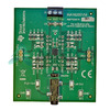 INA1620EVMTexas InstrumentsEVAL MODULE
 INA1620RTWRTexas Instruments
 INA1620RTWTTexas InstrumentsIC AUDIO 2 CIRCUIT 24WQFN
 INA156EA/2K5G4Luminary Micro / Texas InstrumentsIC OPAMP INSTR 550KHZ RRO 8VSSOP
- Emil***rperTech
- Jun 23, 2026

Image may be representation.
See specifications for product details.
See specifications for product details.
- EXPRESS OPTION
- Payment method
INA157UK - BURR-BROWN
- Manufacturer Part Number
- INA157UK
- Manufacturer
- BURR-BROWN
- Allelco Part Number
- 32D-INA157UK
- Warranty
- 1 Year Allelco Warranty - Find out more
- Stock Status:
- 12,260 pcs available, New & Original
- Parts Description
- DAC91001
- Data sheet
- -
- Category
- Integrated Circuits (ICs) > Specialized ICs
- RoHs Status
- Our certification
- In stock: 12260


