

SN74ALVCH16841DGGR (1)
Manufacturer Part Number
SN74ALVCH16841DGGR
Manufacturer
Texas Instruments
Introduction
The SN74ALVCH16841DGGR is a D-Type Transparent Latch designed for high-speed, low-voltage applications in logic latching operations.
Product Features and Performance
Logic Type: D-Type Transparent Latch
Circuit Configuration: 10:10
Output Type: Tri-State
Voltage Supply Range: 1.65V to 3.6V
Independent Circuits: 2
Propagation Delay Time: 1ns
Output Current High, Low: 24mA
Operating Temperature Range: -40°C to 85°C
Mounting Type: Surface Mount
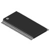
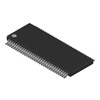
Package: 56-TFSOP (Width 6.10mm)
Product Advantages
High-speed performance with propagation delay of only 1ns
Low voltage operation, suitable for modern low-power applications
Tri-State output for increased flexibility in circuit integration
Dual independent circuits enhance versatility
Key Technical Parameters
Propagation Delay Time: 1ns
Supply Voltage: 1.65V 3.6V
Output Current: 24mA High, 24mA Low
Temperature Operating Range: -40°C to 85°C
Quality and Safety Features
Compliant with industry standards for electronic component safety and performance
Compatibility
Compatible with various logic families due to its wide voltage supply range and Tri-State output functionality
Application Areas
Telecommunications
Computing systems
Data processing
Industrial controls
Product Lifecycle
Status: Active
Not nearing discontinuation and replacements or upgrades are readily available
Several Key Reasons to Choose This Product
Extremely fast performance with minimal propagation delay
Operates effectively across a range of power supply levels
Provides high output current for driving multiple loads
Applicable in a variety of high-demand environments due to its robust operating temperature range
Reliable and durable design supported by Texas Instruments’ reputable manufacturing standards


 SN74ALVCH16901DGGTexas InstrumentsREGISTERED BUS TRANSCEIVER
 SN74ALVCH16835DGVRTexas InstrumentsIC UNIV BUS DVR 18BIT 56TVSOP
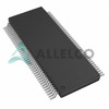 SN74ALVCH16831DBBRTexas InstrumentsIC ADDRESS DRIVER 3.6V 80TSSOP
 SN74ALVCH16835KRTexas InstrumentsIC UNIV BUS DVR 18BIT 56BGA
 SN74ALVCH16901DGGRG4Texas Instruments


