
Manufacturer Part Number
SN74ALVCH16841DL
Manufacturer
Texas Instruments
Introduction
The SN74ALVCH16841DL is a high-performance, voltage-translating 10-bit D-type transparent latch with tri-state outputs. It is designed to provide efficient voltage translation and level shifting between different logic families, enabling seamless integration of components with varying supply voltages.
Product Features and Performance
10-bit D-type transparent latch with tri-state outputs
Supports voltage translation between 1.65V to 3.6V
Propagation delay of only 1ns
High output current capability of 24mA (high and low)
Wide operating temperature range of -40°C to 85°C
Efficient surface-mount package (56-BSSOP)
Product Advantages
Enables seamless voltage translation between logic families
Minimizes power consumption and heat generation
Compact surface-mount package for space-efficient designs
Robust operating temperature range for a wide variety of applications
Key Reasons to Choose This Product
Exceptional performance and efficiency for voltage translation
Reliable and stable operation across a wide range of conditions
Ease of integration with various logic families and system designs
Optimized for space-constrained applications
Quality and Safety Features
Complies with safety standards for electronic components
Rigorous quality control and testing procedures
Backed by Texas Instruments' reputation for reliability and innovation
Compatibility
The SN74ALVCH16841DL is designed to be compatible with a variety of logic families, including CMOS, TTL, and other LVDS/LVPECL-compatible devices.
Application Areas
Digital signal processing
Communication systems
Industrial control and automation
Embedded systems
Military and aerospace applications
Product Lifecycle
The SN74ALVCH16841DL is an active product, currently in production. There are no immediate plans for discontinuation. If you require information about equivalent or alternative models, please contact our sales team through our website for the latest updates and recommendations.
 SN74ALVCH16832DGGRTexas InstrumentsIC ADDRESS DRIVER 3.6V 64TSSOP
 SN74ALVCH16841DLRTexas InstrumentsIC LATCH BUS 20BIT D 3ST 56-SSOP
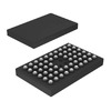 SN74ALVCH16835KRTexas InstrumentsIC UNIV BUS DVR 18BIT 56BGA
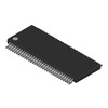 SN74ALVCH16901DGGTexas InstrumentsREGISTERED BUS TRANSCEIVER
 SN74ALVCH16835DGVRTexas InstrumentsIC UNIV BUS DVR 18BIT 56TVSOP
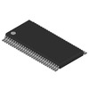 SN74ALVCH16835DGGTexas InstrumentsBUS DRIVER, ALVC/VCX/A SERIES
 SN74ALVCH16841Texas Instruments


