
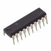
 SN74LVC245ANTexas InstrumentsIC TXRX NON-INVERT 3.6V 20DIP
 SN74LVC245AIPWREPTexas Instruments
 SN74LVC245APWRTexas InstrumentsIC TXRX NON-INVERT 3.6V 20TSSOP
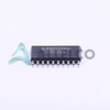 SN74LVC245ANSRTexas InstrumentsIC TXRX NON-INVERT 3.6V 20SO
- Nath***rooks
- Jun 11, 2026
HomeProductsIntegrated Circuits (ICs)Logic - Buffers, Drivers, Receivers, TransceiversSN74LVC245APWE4
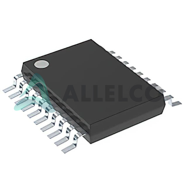
Image may be representation.
See specifications for product details.
See specifications for product details.
- EXPRESS OPTION
- Payment method
SN74LVC245APWE4 - Texas Instruments
- Manufacturer Part Number
- SN74LVC245APWE4
- Manufacturer
- Texas Instruments
- Allelco Part Number
- 98D-SN74LVC245APWE4
- Warranty
- 1 Year Allelco Warranty - Find out more
- Stock Status:
- 12,726 pcs available, New & Original
- Parts Description
- IC TXRX NON-INVERT 3.6V 20TSSOP
- Package
- 20-TSSOP
- Data sheet
-
SN74LVC245APWE4.pdf
HTML Datasheet
SN74LVC245A.pdf
- RoHs Status
- ROHS3 Compliant
- Our certification
- In stock: 12726


