View All

Please refer to the English Version as our Official Version.Return

Europe
France(Français) Germany(Deutsch) Italy(Italia) Russian(русский) Poland(polski) Czech(Čeština) Luxembourg(Lëtzebuergesch) Netherlands(Nederland) Iceland(íslenska) Hungarian(Magyarország) Spain(español) Portugal(Português) Turkey(Türk dili) Bulgaria(Български език) Ukraine(Україна) Greece(Ελλάδα) Israel(עִבְרִית) Sweden(Svenska) Finland(Svenska) Finland(Suomi) Romania(românesc) Moldova(românesc) Slovakia(Slovenská) Denmark(Dansk) Slovenia(Slovenija) Slovenia(Hrvatska) Croatia(Hrvatska) Serbia(Hrvatska) Montenegro(Hrvatska) Bosnia and Herzegovina(Hrvatska) Lithuania(lietuvių) Spain(Português) Switzerland(Deutsch) United Kingdom(English)
Asia/Pacific
Japan(日本語) Korea(한국의) Thailand(ภาษาไทย) Malaysia(Melayu) Singapore(Melayu) Vietnam(Tiếng Việt) Philippines(Pilipino)
Africa, India and Middle East
United Arab Emirates(العربية) Iran(فارسی) Tajikistan(فارسی) India(हिंदी) Madagascar(malaɡasʲ)
South America / Oceania
New Zealand(Maori) Brazil(Português) Angola(Português) Mozambique(Português)
North America
United States(English) Canada(English) Haiti(Ayiti) Mexico(español)
HomeProductsIntegrated Circuits (ICs)Logic - Buffers, Drivers, Receivers, TransceiversSN74LVC245APWRG3-J
SN74LVC245APWRG3-J Image
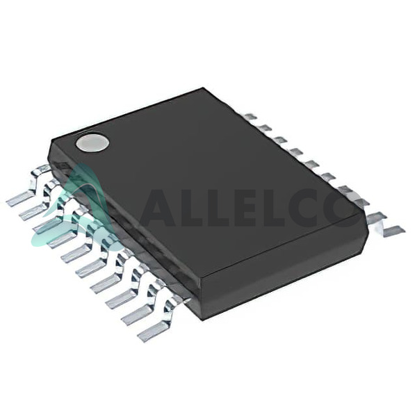
Image may be representation.
See specifications for product details.
EXPRESS OPTION
Payment method

SN74LVC245APWRG3-J - Texas Instruments

Manufacturer Part Number
SN74LVC245APWRG3-J
Manufacturer
Texas Instruments
Allelco Part Number
98D-SN74LVC245APWRG3-J
Warranty
1 Year Allelco Warranty - Find out more
Stock Status:
13,103 pcs available, New & Original
Parts Description
BUS TRANSCEIVER
Package
Bulk
Data sheet
-
RoHs Status
 
Our certification
In stock: 13103
  • Unit Price: $0.142
  • Subtotal: $0.00

Want a better price?
Add to Cart and Submit RFQ now, we'll contact you immediately.

Quantity Unit Price Ext. Price
1+ $0.142 $0.14
200+ $0.055 $11.00
500+ $0.053 $26.50
1000+ $0.052 $52.00
The above prices does not include taxes and freight rates, which will be calculated on the order pages.

Specifications

SN74LVC245APWRG3-J Tech Specifications
Texas Instruments - SN74LVC245APWRG3-J technical specifications, attributes, parameters and parts with similar specifications to Texas Instruments - SN74LVC245APWRG3-J

Product Attribute Attribute Value
Manufacturer Texas Instruments
Series *
Product Attribute Attribute Value
Package Bulk
Base Product Number 74LVC245

Environmental & Export Classifications

ATTRIBUTE DESCRIPTION
RoHs Status Not applicable
Moisture Sensitivity Level (MSL) 3 (168 Hours)
REACH Status Vendor Undefined
ECCN EAR99
HTSUS 8542.39.0001

Frequently Asked Questions(FAQ)

What are the key electrical characteristics of the SN74LVC245APWRG3-J transceiver that influence its suitability for bidirectional bus communication in mixed-voltage systems?
The SN74LVC245APWRG3-J operates over a supply voltage range of 1.65V to 3.6V, enabling it to interface between devices with different logic levels such as 1.8V microcontrollers and 3.3V peripherals. Its 3-state output architecture allows high-impedance states during non-transmission periods, preventing contention on shared data buses. With output drive currents of ±24mA, the device supports driving capacitive loads or multiple inputs without requiring external buffering. These features make it particularly effective in automotive and industrial applications where voltage translation and noise immunity are critical.
How does the propagation delay performance of the SN74LVC245APWRG3-J compare when operating at the lower end versus the upper end of its supply voltage range, and what implications does this have for high-speed system design?
At 1.65V, typical propagation delays increase due to reduced transistor switching speeds compared to operation near 3.6V. For example, a common scenario shows an input-to-output delay rising from approximately 2.1ns at 3.6V to around 3.4ns at 1.65V under standard load conditions. This degradation affects maximum usable clock frequencies in synchronous designs. Engineers must account for this variation when selecting the SN7VC245APWRG3-J in time-critical paths—especially in battery-powered systems where lower voltages extend runtime but reduce speed headroom.
In what scenarios would using the SN74LVC245APWRG3-J be preferable over a dedicated voltage-level translator IC, despite both serving similar functions?
The SN74LVC245APWRG3-J offers built-in direction control and tri-state outputs, making it ideal for bidirectional data bus applications like I²C expansion or parallel memory interfaces. Unlike some level translators that require external enable signals or fixed directionality, this device natively supports automatic flow control based on the DIR pin. Additionally, its integration of eight full-bit transceivers reduces board space and simplifies routing compared to discrete solutions. However, if only partial bit translation is needed or if signal integrity demands strict skew control, a purpose-built translator may offer better performance.
What precautions should be taken when cascading multiple SN74LVC245APWRG3-J devices in a multi-drop configuration to avoid timing violations or signal degradation?
When chaining several SN74LVC245APWRG3-J units along a shared bus, cumulative propagation delays can exceed acceptable thresholds for fast protocols like SPI or parallel memory access. A rule of thumb is to limit chain length so that total round-trip delay remains below 70% of the minimum clock period. Also, ensure proper termination and avoid long stubs from each tap point to prevent reflections. Since each device adds roughly 2–4ns of latency depending on voltage and load, careful path planning and possibly buffer insertion may be necessary in high-speed designs.
How does the Moisture Sensitivity Level (MSL) rating of MSL 1 for the SN74LVC245APWRG3-J impact storage and handling procedures before PCB assembly?
Classified as MSL 1 (unlimited floor life), the SN74LVC245APWRG3-J does not require baking prior to use and can be stored indefinitely under dry conditions. This simplifies inventory management and reduces production costs by eliminating pre-bake steps. However, once the moisture barrier bag is opened, exposure to ambient humidity during soldering must still comply with JEDEC J-STD-020 guidelines—typically within 168 hours of opening for standard reflow profiles. Proper handling ensures reliability and prevents popcorning during thermal stress.
Can the SN74LVC245APWRG3-J reliably interface between a 5V microcontroller and a 3.3V sensor network, and what circuit modifications might be needed?
While the SN74LVC245APWRG3-J supports inputs up to 5.5V (per absolute maximum ratings), direct connection from a 5V system requires caution. Input thresholds scale with VCC; thus, driving a 3.3V-supplied transceiver from 5V may violate valid logic-high recognition if VCC is only 3.3V. One approach is to use a resistive divider or Schmitt-trigger buffers on the 5V side. Alternatively, configure the SN74LVC245APWRG3-J with VCC = 3.3V and ensure upstream drivers meet LVCMOS compatibility. Always verify noise margins under worst-case temperature and process corners.
What role does the DIR pin play in the operation of the SN74LVC245APWRG3-J, and how does incorrect usage lead to bus contention?
The DIR pin controls the direction of data flow: high enables transmission from A to B ports, low from B to A. Misconfiguring this pin during power-up or dynamic reconfiguration can cause both sides to attempt driving simultaneously, resulting in excessive current draw and potential damage. To prevent this, initialize DIR before asserting OE (output enable), and consider adding pull-up/down resistors if the pin floats during reset sequences. In autonomous systems, ensure stable direction logic throughout all operational states to maintain safe bidirectional handshaking.
How does temperature variation across the -40°C to +125°C range affect the output leakage current and overall power consumption of the SN74LVC245APWRG3-J?
Leakage current increases exponentially with temperature—typical values rise from nanoamps at room temperature to microamps at 125°C. For instance, at VCC = 3.6V and TA = 125°C, reverse-biased input leakage might reach 10µA per pin. This contributes to higher quiescent power in always-on applications like automotive ECUs. Designers should factor in these losses when calculating thermal budgets and selecting heatsinks or fan strategies. Derating output loads or disabling unused channels can mitigate self-heating effects in compact layouts.
Are there any known substitution risks when replacing the SN74LVC245APWRG3-J with alternative parts like the SN74LVC245APWT, and how do their package options differ?
The SN74LVC245APWT is functionally equivalent and shares the same pinout and electrical characteristics, making it a direct substitute in most applications. However, packaging differences exist: while both are TSSOP variants, slight dimensional tolerances or lead frame variations could affect solder joint reliability in high-vibration environments. Always confirm mechanical footprint compatibility with your PCB layout. Additionally, check availability and lead times—substitutes may carry longer procurement cycles or regional restrictions impacting supply chain resilience.
What considerations apply when using the SN74LVC245APWRG3-J in hot-swappable USB peripheral designs, given its ESD protection capabilities?
The device includes integrated ESD protection diodes on all pins rated for ±8kV contact discharge per IEC 61000-4-2, which helps survive accidental plug/unplug events. However, USB hot-plug scenarios involve inductive kick and transient surges beyond normal operation. Supplementing with TVS diodes and series resistors improves robustness. Also, ensure OE is asserted only after stable power rails to prevent glitching. Though the SN74LVC245APWRG3-J handles moderate transients well, comprehensive protection networks remain essential for compliance with USB-IF standards.
How does the base product number 74LVC245 relate to the full part code SN74LVC245APWRG3-J, and why might engineers reference the base number when searching for alternatives?
The prefix "SN" denotes Texas Instruments branding, "74LVC245" specifies the core device family, "A" indicates commercial temperature grade, "P" signifies TSSOP package, "W" means tape-and-reel packaging, and "R" is reel size. The suffix "G3-J" includes green/RoHS compliance and Japan-specific marking. Referencing the base number 74LVC245 simplifies cross-referencing across distributors and simplifies searches for compatible substitutes like SN74LVCH245APWT. It abstracts away packaging and environmental details while retaining functional equivalence.
What is the significance of the "PROTOTYPE" designation in the SN74LVC245APWRG3-J description, and how might it affect production deployment decisions?
Labeling as "PROTOTYPE" suggests this variant may lack final qualification data or long-term reliability testing compared to production-grade parts. While suitable for early-stage validation, reliance on it in mass production could introduce unknown failure modes. Engineers should verify with TI’s latest datasheets and request characterization reports before committing to volume orders. If unavailable elsewhere, consider migrating to standard production codes like SN74LVC245APWT after thorough bench testing under expected operating conditions.
How should PCB layout practices be adjusted when routing signals through the SN74LVC245APWRG3-J to minimize crosstalk and skew between its eight data channels?
Maintain matched trace lengths for corresponding A-to-B and B-to-A pairs to preserve timing alignment, especially in synchronous interfaces. Keep adjacent nets orthogonal and separate by ground planes to reduce capacitive coupling. Due to the 20-pin TSSOP footprint, place decoupling capacitors within 1mm of VCC/GND pads to stabilize supply rails during fast transitions. Avoid daisy-chaining multiple devices on shared nets without impedance matching, as the SN74LVC245APWRG3-J’s 3-state outputs can interact unpredictably under contention. Use simulation tools to model signal integrity before finalization.
Does the SN74LVC245APWRG3-J support partial bus isolation during partial system resets, and what design patterns facilitate safe state transitions?
Yes, by controlling the OE pin independently of DIR, individual byte lanes can be isolated while others continue operating. For example, holding OE high disables all outputs regardless of direction, effectively floating the bus. Coupled with weak pull-ups/downs on external lines, this enables graceful subsystem shutdowns. Ensure OE assertion precedes deassertion of VCC to avoid back-powering through ESD diodes. This capability proves valuable in modular systems where only portions need resetting without disrupting neighboring circuitry.

Parts with Similar Specifications

The three parts on the right have similar specifications to Texas Instruments SN74LVC245APWRG3-J

Product Attribute SN74LVC245APWRG3 SN74LVC245APWRG4 SN74LVC245APWR-P SN74LVC245APWR
Part Number SN74LVC245APWRG3 SN74LVC245APWRG4 SN74LVC245APWR-P SN74LVC245APWR
Manufacturer Texas Instruments Texas Instruments Texas Instruments Texas Instruments
Series - - - -
Package - Tape & Reel (TR) Tube Tape & Reel (TR)
Base Product Number - DAC34H84 MAX500 ADS62P42

Customer Reviews

Evaluation: 10 Articles

  • Nath***rooks
    Jun 11, 2026

    Installed this power component in a converter board. Output remained stable under different load conditions and thermal performance was better than expected.

  • Dani***alkerTech
    Jun 1, 2026

    Product works, but setup took more effort than expected. Once configured the MCU ran reliably, although documentation support felt older compared with newer platforms. Fine for maintenance projects.

  • Yuki***aka88
    May 26, 2026

    信号通信プロジェクトでこのRS-485トランシーバーを使用しました。設置は簡単で、長距離ケーブルでも通信は安定していました。消費電力も、以前使用していたものより低くなっています。

  • Stev***aker
    May 20, 2026

    Solid diode for power rectification. Works well in switching circuits.

  • Bran***Lewis
    May 11, 2026

    Compact FPGA with good performance. Suitable for basic signal processing tasks.

  • Oliv***arris
    May 7, 2026

    Reliable I/O expander. Works well in embedded control applications.

  • Jess***Jones
    Apr 17, 2026

    It offers good value for the price, and the specifications match the description. I’ve been using it for two days with no issues, and I’ll definitely buy it again if I need it in the future.

  • Mich***Smith
    Apr 17, 2026

    Shipping was on time, the component pins are neatly aligned, and I tested 10 of them with a multimeter—all readings were within the specified range. Highly recommended.

  • Aman***arris
    Apr 3, 2026

    It was great—the entire process, from placing the order to receiving the package, went very smoothly. The components were consistent, the price was fair, and I had a very pleasant shopping experience.

  • Mike***nch
    Apr 3, 2026

    Better than expected! The resistance and capacitance readings were spot-on, and it passed the test on the first try. The service was reliable, and the packaging was thoughtful—I highly recommend it.

Write a Review

Your Email address will not be published.

Shipment

Delivery Time

In-stock items can be shipped within 24 hours. Some parts will be arranged for delivery within 1-2 days from the date all items arrive at our warehouse. And Allelco ships order once a day at about 17:00, except Sunday. Once the goods are shipped, the estimated delivery time depends on the shipping methods and Delivery destination. The table below shows are the logistic time for some common countries.

Delivery Cost

  1. Use your express account for shipment if you have one.
  2. Use our account for the shipment. Refer to the table below for the approximate charges.
(Different time frame / countries / package size has different price.)

Delivery Method

  1. Global Common Shipment by DHL / UPS / FedEx / TNT / EMS / SF we support.
  2. Others more shipping ways, please get in touch with your customer manager.

Common Countries Logistic Time Reference
Region Country Logistic Time(Day)
America United States 5
Brazil 7
Europe Germany 5
United Kingdom 4
Italy 5
Oceania Australia 6
New Zealand 5
Asia India 4
Japan 4
Middle East Israel 6
DHL & FedEx Shipment Charges Reference
Shipment charges(KG) Reference DHL(USD$)
0.00kg-1.00kg USD$30.00 - USD$60.00
1.00kg-2.00kg USD$40.00 - USD$80.00
2.00kg-3.00kg USD$50.00 - USD$100.00
Note:
The above table is for reference only. There may have some data bias for the uncontrollable factors.
Contact us if you have any questions.
  • QC (Quality Warranty)
  • Payment Support
  • Packaging
  • Certifications & Memberships

QC (Quality Warranty)

Allelco is committed to exceeding customer expectations through customer service excellence, order accuracy, and on-time delivery.
This is achieved through our commitment to the continual improvement of our processes, services, and products.


Strict quality inspection builds a solid foundation for electronic component quality.
  1. Visual inspection
  2. Performance testing and reliability verification
  3. Standardized full-process testing
  4. Precise control of every parameter
We eliminate defective components and ensure the stable operation of electronic devices through professional quality standards.

Payment Support

The payment method can be chosen from the methods shown below: Wire Transfer (T/T, Bank Transfer), Western Union, Credit card, PayPal.
  • HKBea
  • Paypal
  • MasterCard
  • Western-Union
  • VISA
Stable Delivery, Sincere Partnership — Your Faithful Supply Chain Partner
  • Efficient Supply Management
  • Cost-Saving Procurement
  • Fast Sourcing & Delivery
Contact us if you have any questions.

Packaging

Electrostatic Discharge Protection and Handling

All electrostatic-sensitive components are handled in accordance with electrostatic discharge control procedures. The products are hermetically sealed in anti-static safe packaging to prevent electrostatic damage. Appropriate labeling is also applied for identification and traceability. This ensures product integrity during storage, handling and transportation.


ESD

Certifications & Memberships

Third-party certified, strict quality control. Our certification
  • ISO 9001: 2015
  • ISO 13485: 2016
  • ISO 14001: 2015
  • ISO 28000: 2007
  • ISO 45001: 2018
  • GB/T 27922-2011
  • SMTA
  • IPC
  • ESD
  • PSMA
SN74LVC245APWRG3-J Image

SN74LVC245APWRG3-J

Texas Instruments
98D-SN74LVC245APWRG3-J

Want a better price? Add to Cart and Submit RFQ now, we'll contact you immediately.

0 RFQ
Shopping cart (0 Items)
It is empty.
Compare List (0 Items)
It is empty.
Feedback

Your feedback matters! At Allelco, we value the user experience and strive to improve it constantly.
Please share your comments with us via our feedback form, and we'll respond promptly.
Thank you for choosing Allelco.

Subject
E-mail
Comments
Captcha
Drag or click to upload file
Upload File
types: .xls, .xlsx, .doc, .docx, .jpg, .png and .pdf.
Max file size: 10MB