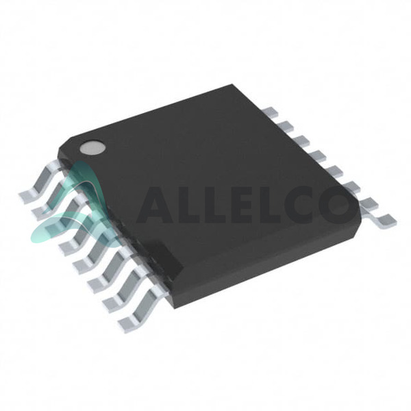
View All

Please refer to the English Version as our Official Version.Return

Europe
France(Français) Germany(Deutsch) Italy(Italia) Russian(русский) Poland(polski) Czech(Čeština) Luxembourg(Lëtzebuergesch) Netherlands(Nederland) Iceland(íslenska) Hungarian(Magyarország) Spain(español) Portugal(Português) Turkey(Türk dili) Bulgaria(Български език) Ukraine(Україна) Greece(Ελλάδα) Israel(עִבְרִית) Sweden(Svenska) Finland(Svenska) Finland(Suomi) Romania(românesc) Moldova(românesc) Slovakia(Slovenská) Denmark(Dansk) Slovenia(Slovenija) Slovenia(Hrvatska) Croatia(Hrvatska) Serbia(Hrvatska) Montenegro(Hrvatska) Bosnia and Herzegovina(Hrvatska) Lithuania(lietuvių) Spain(Português) Switzerland(Deutsch) United Kingdom(English)
Asia/Pacific
Japan(日本語) Korea(한국의) Thailand(ภาษาไทย) Malaysia(Melayu) Singapore(Melayu) Vietnam(Tiếng Việt) Philippines(Pilipino)
Africa, India and Middle East
United Arab Emirates(العربية) Iran(فارسی) Tajikistan(فارسی) India(हिंदी) Madagascar(malaɡasʲ)
South America / Oceania
New Zealand(Maori) Brazil(Português) Angola(Português) Mozambique(Português)
North America
United States(English) Canada(English) Haiti(Ayiti) Mexico(español)
HomeProductsIntegrated Circuits (ICs)Logic - Signal Switches, Multiplexers, DecodersSN74LVC257ADBR
SN74LVC257ADBR Image
Image may be representation.
See specifications for product details.
EXPRESS OPTION
Payment method

SN74LVC257ADBR - Texas Instruments

Manufacturer Part Number
SN74LVC257ADBR
Manufacturer
Texas Instruments
Allelco Part Number
32D-SN74LVC257ADBR
Warranty
1 Year Allelco Warranty - Find out more
Stock Status:
172,990 pcs available, New & Original
Parts Description
IC MULTIPLEXER 4 X 2:1 16SSOP
Package
16-SSOP
Data sheet
SN74LVC257ADBR.pdf
RoHs Status
ROHS3 Compliant
Our certification
In stock: 172990
  • Unit Price: $0.394
  • Subtotal: $0.00

Want a better price?
Add to Cart and Submit RFQ now, we'll contact you immediately.

Quantity Unit Price Ext. Price
1+ $0.394 $0.39
200+ $0.153 $30.60
500+ $0.147 $73.50
1000+ $0.145 $145.00
The above prices does not include taxes and freight rates, which will be calculated on the order pages.

Specifications

SN74LVC257ADBR Tech Specifications
Texas Instruments - SN74LVC257ADBR technical specifications, attributes, parameters and parts with similar specifications to Texas Instruments - SN74LVC257ADBR

Product Attribute Attribute Value
Manufacturer Texas Instruments
Voltage Supply Source Single Supply
Voltage - Supply 1.65V ~ 3.6V
Type Multiplexer
Supplier Device Package 16-SSOP
Series 74LVC
Package / Case 16-SSOP (0.209', 5.30mm Width)
Product Attribute Attribute Value
Package Tape & Reel (TR)
Operating Temperature -40°C ~ 85°C
Mounting Type Surface Mount
Independent Circuits 1
Current - Output High, Low 24mA, 24mA
Circuit 4 x 2:1
Base Product Number 74LVC257

Environmental & Export Classifications

ATTRIBUTE DESCRIPTION
RoHs Status ROHS3 Compliant
Moisture Sensitivity Level (MSL) 1 (Unlimited)
REACH Status REACH Unaffected
ECCN EAR99
HTSUS 8542.39.0001

Parts Introduction

SN74LVC257ADBR Image
SN74LVC257ADBR (1)

Manufacturer Part Number

SN74LVC257ADBR

Manufacturer

Texas Instruments

Introduction

The SN74LVC257ADBR is a 4-channel, 2:1 multiplexer from Texas Instruments designed for efficient signal routing in electronic systems.

Product Features and Performance

4-channel 2:1 multiplexer

Single independent circuit operation

Output Current: High and low levels at 24mA each

Voltage Supply Range: 1.65V to 3.6V

Operating Temperature Range: -40°C to 85°C

Product Advantages

High signal integrity due to controlled voltage levels

Optimal performance in diverse temperature environments

Compact size for space-sensitive applications

Key Technical Parameters

Circuit Configuration: 4 x 2:1

Current Output High, Low: 24mA, 24mA

Voltage Supply: 1.65V ~ 3.6V

Operating Temperature: -40°C ~ 85°C

Quality and Safety Features

Ensured reliability and performance consistency

Compliant with industry-standard safety and quality norms

Compatibility

Compatible with Single Supply operations

Application Areas

Designed for data signal routing in telecommunications

Applicable in computing systems

Utilizable in consumer electronics and industrial applications

Product Lifecycle

Status: Active

Supported with updates and potential future enhancements

Several Key Reasons to Choose This Product

Precision in 2:1 signal multiplexing

Robust temperature tolerance enabling wide-range usage

High output current support for stronger signal driving

Surface mount package for efficient PCB design accommodation

Long product lifecycle ensuring operational continuity and support

Sourced from Texas Instruments, a reputable semiconductor manufacturer

Frequently Asked Questions(FAQ)

What are the key electrical characteristics of the SN74LVC257ADBR multiplexer that influence signal integrity in high-speed digital systems?
The SN74LVC257ADBR supports a supply voltage range of 1.65V to 3.6V, which enables compatibility with both low-voltage logic families and legacy 3.3V systems. Its output current capability of ±24mA allows for robust fan-out to multiple loads without requiring additional buffering. These characteristics make it suitable for applications where power efficiency and noise margin are critical, such as battery-powered devices or dense PCB layouts. When operating near the lower end of the supply range, designers must ensure that propagation delay remains within acceptable bounds for their clock frequency.
How does the pin configuration of the SN74LVC257ADBR affect board layout and routing complexity in space-constrained designs?
The SN74LVC257ADBR is housed in a 16-lead SSOP package with a body width of 5.30mm, offering a compact footprint ideal for portable electronics. The standard pinout arranges control inputs (such as enable and select lines) and data paths in a logical sequence, reducing crosstalk risk when following manufacturer-recommended routing guidelines. However, due to the close spacing between adjacent pins, careful attention to trace impedance and return path planning is necessary to maintain signal integrity, especially in high-frequency switching applications.
Can the SN74LVC257ADBR be used in mixed-voltage environments where 1.8V logic interfaces with 3.3V peripherals?
Yes, the SN74LVC257ADBR supports single-supply operation from 1.65V to 3.6V, enabling level-shifting functionality across this entire range. It features 5.5V-tolerant I/Os on all pins when powered at VCC ≤ 3.6V, allowing direct connection to 5V systems without external clamping diodes. This makes it well-suited for bridging communication buses between microcontrollers running at 1.8V and sensors or displays operating at 3.3V, provided that input voltages do not exceed absolute maximum ratings.
What thermal considerations should engineers evaluate when deploying the SN74LVC257ADBR in continuous-operation industrial equipment?
Operating the SN74LVC257ADBR over its full temperature range (-40°C to 85°C) requires assessing junction temperature rise under worst-case ambient conditions. While the device itself dissipates minimal power due to low quiescent current, simultaneous high-output current (up to 24mA per channel) and elevated ambient temperatures can lead to localized heating. In densely populated boards, adequate copper pour and thermal vias should be implemented to dissipate heat effectively and prevent long-term reliability degradation.
How does the propagation delay of the SN7VC257ADBR compare to other quad 2-to-1 multiplexers like the SN74LVT257 or CD74HC257 when driving capacitive loads?
The SN74LVC257ADBR typically exhibits propagation delays of approximately 3.2 ns at 2.5V supply and room temperature, making it significantly faster than many CMOS variants such as the CD74HC257, which may exceed 10 ns under similar conditions. Compared to the SN74LVT257—a higher-drive version optimized for 3.3V systems—the LVC family trades slightly increased delay for broader voltage compatibility and reduced power consumption, offering a favorable balance for modern low-power embedded designs.
Is the SN74LVC257ADBR suitable for use in automotive-grade systems requiring AEC-Q100 qualification?
No, the SN74LVC257ADBR is not qualified to AEC-Q100 standards and is intended for commercial and industrial applications only. Its specified operating temperature range (-40°C to 85°C) covers most industrial environments but falls short of the -40°C to +125°C requirement common in automotive electronics. For safety-critical or harsh-environment automotive subsystems, alternative components explicitly marked as AEC-Q100 compliant should be selected instead.
What precautions are necessary when cascading multiple SN74LVC257ADBR devices to increase channel count?
When cascading SN74LVC257ADBR units, attention must be paid to timing alignment between select lines and data outputs to avoid race conditions. Each device has independent enable and selection logic, so clock synchronization across stages is essential. Additionally, loading effects from downstream inputs can increase effective capacitance on output nodes, potentially degrading rise/fall times and increasing skew. Designers should simulate worst-case load combinations and verify functional margins using IBIS models or SPICE simulations.
How does the Moisture Sensitivity Level (MSL) rating of MSL 1 impact handling and storage procedures for SN74LVC257ADBR components?
With an MSL rating of 1, the SN74LVC257ADBR is considered non-hygroscopic and poses no moisture-related reliability risks during normal handling. It can be stored indefinitely at room temperature and humidity without requiring bake-out before reflow soldering. This simplifies inventory management and reduces manufacturing overhead compared to higher-MSL parts, making it ideal for high-volume production environments.
What design constraints arise from the SN74LVC257ADBR’s input threshold behavior when interfacing with TTL-compatible signals?
The SN74LVC257ADBR uses Schmitt-trigger inputs on some variants, providing hysteresis that helps reject noise on control lines. However, at the lower end of its supply range (e.g., 1.8V), the VIH(min) threshold increases proportionally, meaning that legacy 5V TTL levels may still be recognized correctly thanks to 5.5V tolerance. Still, care must be taken when driving from lower-voltage TTL-like sources to ensure logic-high levels exceed VIH specifications across all operating conditions.
How does package parasitics in the 16-SSOP form factor influence high-impedance node stability in the SN74LVC257ADBR?
The small outline SSOP package presents modest parasitic inductance and capacitance between leads, which generally do not affect DC operation. However, in applications involving high-Z tristate control or slow-switching analog signals, leakage currents through ESD protection diodes can become significant if unused inputs float. To prevent latch-up or unintended conduction, all unused data inputs should be tied to VCC or GND via appropriate pull-up/down resistors based on application requirements.
What trade-offs exist between using the SN74LVC257ADBR versus FPGA-based soft-multiplexer implementations in prototyping scenarios?
The SN74LVC257ADBR offers deterministic timing, predictable power consumption, and simplified firmware development compared to FPGA-based solutions, which introduce software latency and require resource allocation. However, FPGA implementations provide reconfigurability and eliminate discrete component count, benefiting rapid iteration. For final production runs where speed and reliability matter more than flexibility, the SN74LVC257ADBR delivers better cost efficiency and shorter time-to-market.
Does the SN74LVC257ADBR support hot-swapping or live insertion into powered backplanes?
Hot-swapping capability depends on external circuitry rather than inherent device features. While the SN74LVC257ADBR has built-in ESD protection up to ±2kV HBM, connecting its outputs directly to unpowered loads during insertion can cause reverse current flow through protection diodes and potential damage. Implementing series resistors or using hot-swap controllers is recommended for backplane applications to limit inrush current and protect both the IC and connected peripherals.
How does the supply current consumption of the SN74LVC257ADBR scale with operating frequency and number of active channels?
The SN74LVC257ADBR exhibits very low static supply current (typically < 1 µA at 3.3V), making it highly efficient in sleep-mode applications. Dynamic current scales linearly with switching activity: each active 2:1 mux consumes roughly 1–2 mA per MHz of switching frequency, assuming typical capacitive loads. Therefore, total power dissipation is minimized when only one or two channels are frequently toggled while others remain disabled.
What compliance documentation is available for the SN74LVC257ADBR regarding environmental and regulatory standards?
The SN74LVC257ADBR complies with RoHS3 directives, confirming absence of restricted substances such as lead, mercury, and cadmium. It is also REACH unaffected and classified under ECCN EAR99, indicating unrestricted export eligibility under most jurisdictions. Full compliance certificates and test reports are available through Texas Instruments upon request, supporting audit trails for aerospace, medical, and consumer electronics projects requiring formal documentation.
In what scenarios would replacing the SN74LVC257ADBR with a solid-state relay or analog switch be preferable?
Solid-state relays or analog switches become advantageous when isolating galvanically separated circuits or handling AC signals beyond digital logic levels. The SN74LVC257ADBR is designed for clean digital routing and cannot tolerate AC mains or inductive loads directly. If isolation, bidirectional signal handling, or voltage translation beyond 3.6V is required, alternatives like the MAX4624 or optocoupler-based multiplexers would offer superior performance and safety margins.

Parts with Similar Specifications

The three parts on the right have similar specifications to Texas Instruments SN74LVC257ADBR

Product Attribute SN74LVC257ADBRE4 SN74LVC257ADBRG4 SN74LVC257ADB SN74LVC257ADR
Part Number SN74LVC257ADBRE4 SN74LVC257ADBRG4 SN74LVC257ADB SN74LVC257ADR
Manufacturer Luminary Micro / Texas Instruments Luminary Micro / Texas Instruments Texas Instruments Texas Instruments
Current - Output High, Low - - - -
Independent Circuits - - - -
Series - - - -
Mounting Type - Surface Mount Through Hole Surface Mount
Voltage - Supply - - - -
Package - Tape & Reel (TR) Tube Tape & Reel (TR)
Supplier Device Package - 196-NFBGA (12x12) 16-PDIP 64-VQFN (9x9)
Circuit - - - -
Voltage Supply Source - - - -
Base Product Number - DAC34H84 MAX500 ADS62P42
Type - - - -
Package / Case - 196-LFBGA 16-DIP (0.300', 7.62mm) 64-VFQFN Exposed Pad
Operating Temperature - -40°C ~ 85°C 0°C ~ 70°C -40°C ~ 85°C

SN74LVC257ADBR Datasheet PDF

Download SN74LVC257ADBR pdf datasheets and Texas Instruments documentation for SN74LVC257ADBR - Texas Instruments.

Datasheets
Cylindrical Battery Holders.pdf
HTML Datasheet
SN54LVC257A, SN74LVC257A.pdf

Customer Reviews

Evaluation: 10 Articles

  • Nath***rooks
    Jun 11, 2026

    Installed this power component in a converter board. Output remained stable under different load conditions and thermal performance was better than expected.

  • Dani***alkerTech
    Jun 1, 2026

    Product works, but setup took more effort than expected. Once configured the MCU ran reliably, although documentation support felt older compared with newer platforms. Fine for maintenance projects.

  • Yuki***aka88
    May 26, 2026

    信号通信プロジェクトでこのRS-485トランシーバーを使用しました。設置は簡単で、長距離ケーブルでも通信は安定していました。消費電力も、以前使用していたものより低くなっています。

  • Stev***aker
    May 20, 2026

    Solid diode for power rectification. Works well in switching circuits.

  • Bran***Lewis
    May 11, 2026

    Compact FPGA with good performance. Suitable for basic signal processing tasks.

  • Oliv***arris
    May 7, 2026

    Reliable I/O expander. Works well in embedded control applications.

  • Jess***Jones
    Apr 17, 2026

    It offers good value for the price, and the specifications match the description. I’ve been using it for two days with no issues, and I’ll definitely buy it again if I need it in the future.

  • Mich***Smith
    Apr 17, 2026

    Shipping was on time, the component pins are neatly aligned, and I tested 10 of them with a multimeter—all readings were within the specified range. Highly recommended.

  • Aman***arris
    Apr 3, 2026

    It was great—the entire process, from placing the order to receiving the package, went very smoothly. The components were consistent, the price was fair, and I had a very pleasant shopping experience.

  • Mike***nch
    Apr 3, 2026

    Better than expected! The resistance and capacitance readings were spot-on, and it passed the test on the first try. The service was reliable, and the packaging was thoughtful—I highly recommend it.

Write a Review

Your Email address will not be published.

Shipment

Delivery Time

In-stock items can be shipped within 24 hours. Some parts will be arranged for delivery within 1-2 days from the date all items arrive at our warehouse. And Allelco ships order once a day at about 17:00, except Sunday. Once the goods are shipped, the estimated delivery time depends on the shipping methods and Delivery destination. The table below shows are the logistic time for some common countries.

Delivery Cost

  1. Use your express account for shipment if you have one.
  2. Use our account for the shipment. Refer to the table below for the approximate charges.
(Different time frame / countries / package size has different price.)

Delivery Method

  1. Global Common Shipment by DHL / UPS / FedEx / TNT / EMS / SF we support.
  2. Others more shipping ways, please get in touch with your customer manager.

Common Countries Logistic Time Reference
Region Country Logistic Time(Day)
America United States 5
Brazil 7
Europe Germany 5
United Kingdom 4
Italy 5
Oceania Australia 6
New Zealand 5
Asia India 4
Japan 4
Middle East Israel 6
DHL & FedEx Shipment Charges Reference
Shipment charges(KG) Reference DHL(USD$)
0.00kg-1.00kg USD$30.00 - USD$60.00
1.00kg-2.00kg USD$40.00 - USD$80.00
2.00kg-3.00kg USD$50.00 - USD$100.00
Note:
The above table is for reference only. There may have some data bias for the uncontrollable factors.
Contact us if you have any questions.
  • QC (Quality Warranty)
  • Payment Support
  • Packaging
  • Certifications & Memberships

QC (Quality Warranty)

Allelco is committed to exceeding customer expectations through customer service excellence, order accuracy, and on-time delivery.
This is achieved through our commitment to the continual improvement of our processes, services, and products.


Strict quality inspection builds a solid foundation for electronic component quality.
  1. Visual inspection
  2. Performance testing and reliability verification
  3. Standardized full-process testing
  4. Precise control of every parameter
We eliminate defective components and ensure the stable operation of electronic devices through professional quality standards.

Payment Support

The payment method can be chosen from the methods shown below: Wire Transfer (T/T, Bank Transfer), Western Union, Credit card, PayPal.
  • HKBea
  • Paypal
  • MasterCard
  • Western-Union
  • VISA
Stable Delivery, Sincere Partnership — Your Faithful Supply Chain Partner
  • Efficient Supply Management
  • Cost-Saving Procurement
  • Fast Sourcing & Delivery
Contact us if you have any questions.

Packaging

Electrostatic Discharge Protection and Handling

All electrostatic-sensitive components are handled in accordance with electrostatic discharge control procedures. The products are hermetically sealed in anti-static safe packaging to prevent electrostatic damage. Appropriate labeling is also applied for identification and traceability. This ensures product integrity during storage, handling and transportation.


ESD

Certifications & Memberships

Third-party certified, strict quality control. Our certification
  • ISO 9001: 2015
  • ISO 13485: 2016
  • ISO 14001: 2015
  • ISO 28000: 2007
  • ISO 45001: 2018
  • GB/T 27922-2011
  • SMTA
  • IPC
  • ESD
  • PSMA
SN74LVC257ADBR Image

SN74LVC257ADBR

Texas Instruments
32D-SN74LVC257ADBR

Want a better price? Add to Cart and Submit RFQ now, we'll contact you immediately.

0 RFQ
Shopping cart (0 Items)
It is empty.
Compare List (0 Items)
It is empty.
Feedback

Your feedback matters! At Allelco, we value the user experience and strive to improve it constantly.
Please share your comments with us via our feedback form, and we'll respond promptly.
Thank you for choosing Allelco.

Subject
E-mail
Comments
Captcha
Drag or click to upload file
Upload File
types: .xls, .xlsx, .doc, .docx, .jpg, .png and .pdf.
Max file size: 10MB