
SN74LVC257ADR (1)
Manufacturer Part Number
SN74LVC257ADR
Manufacturer
Texas Instruments
Introduction
The SN74LVC257ADR is a multiplexer from the 74LVC series, designed for logic signal switching. It is suitable for applications requiring multiple data selection and data routing based on logic control signals.
Product Features and Performance
Type: Multiplexer
Circuit Configuration: 4 x 2:1
Independent Circuits: One
Output Current: High 24mA, Low 24mA
Supply Voltage Range: 1.65V to 3.6V
Operating Temperature: -40°C to 85°C
Mounting Type: Surface Mount
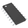
Package Type: 16-SOIC
Product Advantages
High Switching Speed
Low Power Consumption
Wide Operating Temperature Range
Compact Surface Mount Package
Key Technical Parameters
Output Current Capability: 24mA both High and Low
Voltage Supply Range: 1.65V to 3.6V
Minimum Operating Temperature: -40°C
Maximum Operating Temperature: 85°C
Package: 16-SOIC
Quality and Safety Features
Robust Surface Mount Package
Designed to Meet or Exceed Industry Standards for Safety and Performance
Compatibility
Compatible with Single Supply Voltage Systems
Application Areas
Data Routing in Telecommunication
Signal Gating in Data Acquisition Systems
Multiplexing for Input/Output Interfaces in Embedded Systems
Product Lifecycle
Status: Active
No immediate plans for discontinuation, replacements, or upgrades are announced.
Several Key Reasons to Choose This Product
Efficient Data Routing Capabilities
Low Power Draw Enhancing System Longevity
High Reliability Under Wide Temperature Ranges
Easily Integrates into Various Circuit Designs
Consistent Performance with Single Supply Voltage Operation


 SN74LVC245AZQNRTexas InstrumentsIC TXRX NON-INVERT 3.6V 20BGA
 SN74LVC257APWRE4Texas InstrumentsIC MULTIPLEXER 4 X 2:1 16TSSOP
 SN74LVC257APWRTexas InstrumentsIC MULTIPLEXER 4 X 2:1 16TSSOP
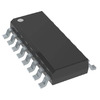 SN74LVC257ANSRTexas InstrumentsIC MULTIPLEXER 4 X 2:1 16SO
 SN74LVC245DBLETexas InstrumentsBUS TRANSCEIVER
 SN74LVC257ADBTexas InstrumentsMUX, 2 LINE INPUT


