
Manufacturer Part Number
SN74LVC257AD
Manufacturer
Texas Instruments
Introduction
The SN74LVC257AD is a 4-bit dual 2-to-1 multiplexer with a high-impedance 3-state output. It is designed for use in applications where low power, high speed, and high-density logic functions are required.
Product Features and Performance
4-bit dual 2-to-1 multiplexer with 3-state outputs
High-speed operation: typical propagation delay of 5.5 ns
Low power consumption: typical ICC of 2 μA
Supports single 1.65V to 3.6V power supply
Wide operating temperature range: -40°C to 85°C
Latch-up performance exceeds 100 mA per JESD 78 Class II
Product Advantages
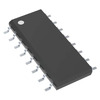
Compact and space-saving design with 16-SOIC package
Versatile functionality for various logic applications
Low power consumption for energy-efficient systems
Wide voltage and temperature range for diverse use cases
Key Reasons to Choose This Product
High-performance multiplexing with low power and fast switching
Reliable and robust design for demanding applications
Compatibility with a wide range of system voltages and environments
Cost-effective solution for space-constrained designs
Quality and Safety Features
ESD protection exceeding 2 kV per JESD 22-A114
Latch-up immunity testing per JESD 78 Class II
Compatibility
Compatible with 3.3V and 5V logic systems
Can be used in a variety of digital electronics and embedded systems
Application Areas
Digital logic circuits
Data acquisition and processing
Embedded systems
Industrial automation and control
Product Lifecycle
The SN74LVC257AD is an active and currently available product from Texas Instruments. There are no direct equivalent or alternative models announced at this time. For the latest information or to inquire about product availability, please contact our website's sales team.
 SN74LVC257ADRG4Texas InstrumentsIC MULTIPLEXER 4 X 2:1 16SOIC
 SN74LVC257ADBRTexas InstrumentsIC MULTIPLEXER 4 X 2:1 16SSOP
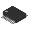 SN74LVC245DBLETexas InstrumentsBUS TRANSCEIVER
 SN74LVC245ARGYRTexas InstrumentsIC TXRX NON-INVERT 3.6V 20VQFN
 SN74LVC257ADBTexas InstrumentsMUX, 2 LINE INPUT
 SN74LVC245AZQNRTexas InstrumentsIC TXRX NON-INVERT 3.6V 20BGA
 SN74LVC245AQPWRHTTexas InstrumentsPROTOTYPE


