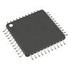


ATMEGA1284P-AU (1)
Manufacturer Part Number
ATMEGA1284P-AU
Manufacturer
Microchip Technology
Introduction
High-performance, low-power Atmel AVR 8-bit microcontroller

ATMEGA1284P-AU (2)
Product Features and Performance
8-bit AVR core
Up to 20MHz operating speed
32 programmable I/O lines
128KB in-system self-programmable flash
4KB EEPROM
16KB SRAM
In-circuit debugging support
Product Advantages
Large memory capacity in its class
Extensive I/O options with 32 programmable pins
Supports high-speed SPI for data transfer
Versatile power management options
Robust PWM and timer/counters
Key Technical Parameters
Core Size: 8-Bit
Speed: 20MHz
Connectivity: I2C, SPI, UART/USART
Program Memory Size: 128KB flash
EEPROM Size: 4KB
RAM Size: 16KB
Voltage Supply: 1.8V to 5.5V
Data Converters: 8-channel, 10-bit A/D
Operating Temperature: -40°C to 85°C
Quality and Safety Features
Brown-out detect and reset
Programmable watch-dog timer with internal oscillator
Power-on reset circuit

ATMEGA1284P-AU (3)
Compatibility
Supports interfacing with I2C, SPI, and UART/USART devices
44-TQFP surface mount package for compatibility with standard PCB assembly
Application Areas
Consumer electronics
Industrial automation
Automotive applications
Internet of Things (IoT) devices
Product Lifecycle
Status: Active
Continuously supported with potential for next-generation upgrades
Several Key Reasons to Choose This Product
Advanced RISC architecture for efficient processing
Improves system reliability with integrated safety features
Flexible and power-efficient design suitable for battery-operated systems
Wide operating voltage and temperature range to suit various environments
Extensive memory and connectivity features add value for complex applications


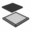 ATMEGA1281V-8MURMicrochip TechnologyIC MCU 8BIT 128KB FLASH 64QFN
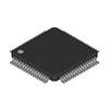 ATMEGA1281V-8AURAtmelIC MCU 8BIT 128KB FLASH 64TQFP
 ATMEGA1284-AUMicrochip
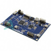 ATMEGA1284P-XPLDMicrochip TechnologyMEGA-1284P XPLAINED ATMEGA1284P
 ATMEGA1284-PUMicrochip TechnologyIC MCU 8BIT 128KB FLASH 40DIP
 ATMEGA1284-AURMicrochip
 ATMEGA1284PMUAtmel


