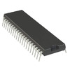
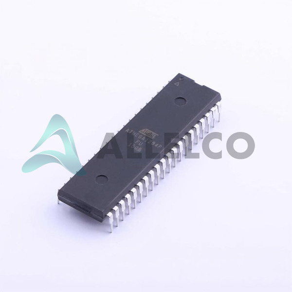
View All

Please refer to the English Version as our Official Version.Return

Europe
France(Français) Germany(Deutsch) Italy(Italia) Russian(русский) Poland(polski) Czech(Čeština) Luxembourg(Lëtzebuergesch) Netherlands(Nederland) Iceland(íslenska) Hungarian(Magyarország) Spain(español) Portugal(Português) Turkey(Türk dili) Bulgaria(Български език) Ukraine(Україна) Greece(Ελλάδα) Israel(עִבְרִית) Sweden(Svenska) Finland(Svenska) Finland(Suomi) Romania(românesc) Moldova(românesc) Slovakia(Slovenská) Denmark(Dansk) Slovenia(Slovenija) Slovenia(Hrvatska) Croatia(Hrvatska) Serbia(Hrvatska) Montenegro(Hrvatska) Bosnia and Herzegovina(Hrvatska) Lithuania(lietuvių) Spain(Português) Switzerland(Deutsch) United Kingdom(English)
Asia/Pacific
Japan(日本語) Korea(한국의) Thailand(ภาษาไทย) Malaysia(Melayu) Singapore(Melayu) Vietnam(Tiếng Việt) Philippines(Pilipino)
Africa, India and Middle East
United Arab Emirates(العربية) Iran(فارسی) Tajikistan(فارسی) India(हिंदी) Madagascar(malaɡasʲ)
South America / Oceania
New Zealand(Maori) Brazil(Português) Angola(Português) Mozambique(Português)
North America
United States(English) Canada(English) Haiti(Ayiti) Mexico(español)
HomeProductsIntegrated Circuits (ICs)Embedded - MicrocontrollersATMEGA1284P-PU
ATMEGA1284P-PU Image
Image may be representation.
See specifications for product details.
EXPRESS OPTION
Payment method

ATMEGA1284P-PU - Microchip Technology

Manufacturer Part Number
ATMEGA1284P-PU
Manufacturer
Microchip Technology
Allelco Part Number
32D-ATMEGA1284P-PU
Warranty
1 Year Allelco Warranty - Find out more
Stock Status:
6,594 pcs available, New & Original
Parts Description
IC MCU 8BIT 128KB FLASH 40DIP
Package
40-PDIP
Data sheet
ATMEGA1284P-PU.pdf
RoHs Status
ROHS3 Compliant
Our certification
In stock: 6594

Required fields are indicated by an asterisk (*)
Please send RFQ, we will respond immediately.

Quantity

Specifications

ATMEGA1284P-PU Tech Specifications
Microchip Technology - ATMEGA1284P-PU technical specifications, attributes, parameters and parts with similar specifications to Microchip Technology - ATMEGA1284P-PU

Product Attribute Attribute Value
Manufacturer Microchip Technology
Voltage - Supply (Vcc/Vdd) 1.8V ~ 5.5V
Supplier Device Package 40-PDIP
Speed 20MHz
Series AVR® ATmega
RAM Size 16K x 8
Program Memory Type FLASH
Program Memory Size 128KB (64K x 16)
Peripherals Brown-out Detect/Reset, POR, PWM, WDT
Package / Case 40-DIP (0.600', 15.24mm)
Package Tube
Product Attribute Attribute Value
Oscillator Type Internal
Operating Temperature -40°C ~ 85°C (TA)
Number of I/O 32
Mounting Type Through Hole
EEPROM Size 4K x 8
Data Converters A/D 8x10b
Core Size 8-Bit
Core Processor AVR
Connectivity I²C, SPI, UART/USART
Base Product Number ATMEGA1284

Environmental & Export Classifications

ATTRIBUTE DESCRIPTION
RoHs Status ROHS3 Compliant
Moisture Sensitivity Level (MSL) 1 (Unlimited)
REACH Status REACH Unaffected
ECCN EAR99
HTSUS 8542.31.0001

Parts Introduction

ATMEGA1284P-PU Image
ATMEGA1284P-PU (1)

Manufacturer Part Number

ATMEGA1284P-PU

Manufacturer

Microchip Technology

Introduction

ATMEGA1284P-PU is an 8-bit high-performance microcontroller of the AVR® ATmega series designed for advanced embedded applications.

Product Features and Performance

Enhanced RISC architecture

AVR Core running at up to 20MHz

128KB of in-system programmable flash

In-built 8-channel 10-bit A/D converter

Up to 32 programmable I/O lines

Advanced power-saving features

Product Advantages

Large program memory space for complex applications

Rich set of peripherals enabling versatile use cases

High integration reduces system component count

Robust design with internal protection features

ATMEGA1284P-PU Image
ATMEGA1284P-PU (2)

Key Technical Parameters

Core Size: 8-Bit

Speed: 20MHz

Connectivity: I2C, SPI, UART/USART

Program Memory Size: 128KB (64K x 16)

EEPROM Size: 4K x 8

RAM Size: 16K x 8

Voltage - Supply: 1.8V ~ 5.5V

Operating Temperature: -40°C ~ 85°C

Quality and Safety Features

Brown-out Detect/Reset

Power-on Reset

Watchdog Timer with separate On-chip Oscillator

Lock bits for software security

Compatibility

Compatible with a broad range of AVR development tools and software

Supports migration to other AVR microcontrollers

Application Areas

Industrial control systems

Automotive applications

Internet of things (IoT) devices

Consumer electronics

Medical devices

Product Lifecycle

Product status: Active

Not nearing discontinuation; replacements or upgrades continuously developed and available

Several Key Reasons to Choose This Product

High computation power for complex algorithms

Extensive interfacing capabilities enhance hardware scalability

Flexible use in various temperature circumstances between -40°C to 85°C

Availability of development tools and software libraries for quick deployment

Reliable performance ensured by quality and safety features

Supports through-hole mounting for easy prototyping and repairs

Frequently Asked Questions(FAQ)

What are the key differences in power consumption and performance between the ATMEGA1284P-PU and other AVR microcontrollers when operating at 5V versus 3.3V, and how does this impact battery-powered design decisions?
The ATMEGA1284P-PU supports a wide voltage range of 1.8V to 5.5V, allowing operation at both 3.3V and 5V. While exact current draw varies with clock speed and peripherals, running at lower voltages significantly reduces dynamic power consumption due to the quadratic relationship with supply voltage (P ∝ V²). At 3.3V and 20MHz, the device draws approximately 6–8 mA, whereas at 5V it may increase to 10–12 mA under similar conditions. This makes the ATMEGA1284P-PU more suitable for 3.3V battery applications such as Li-ion or alkaline-powered systems where extended runtime is critical. Designers should consider voltage scaling to balance performance needs with energy efficiency.
How does the internal oscillator accuracy and startup behavior of the ATMEGA1284P-PU affect timing-sensitive applications like UART baud rate generation or real-time clock implementations?
The ATMEGA1284P-PU includes an internal calibrated 16 MHz RC oscillator with typical accuracy of ±1% over temperature and voltage, though uncalibrated units can vary up to ±10%. This variability impacts precise baud rate generation—for example, a 9600 baud rate derived from an uncalibrated internal oscillator may result in actual rates ranging from ~8640 to 10560 baud, leading to communication errors. For reliable UART operation, external crystal oscillators are recommended. In RTC applications, accumulated timing drift over time may exceed acceptable limits without periodic calibration using features like the built-in calibration registers or external reference.
When selecting between the ATMEGA1284P-PU and alternative microcontrollers with similar flash sizes, what trade-offs exist in terms of peripheral integration, memory architecture, and I/O availability for compact embedded designs?
Compared to many 8-bit MCUs with 128KB flash, the ATMEGA1284P-PU offers a balanced mix of 32 general-purpose I/O pins, integrated ADC, PWM channels, and standard connectivity (SPI, I2C, USART), reducing reliance on external components. Its Harvard architecture separates program and data memory spaces, improving throughput compared to von Neumann-based alternatives. However, some competitors offer higher core frequencies or additional peripherals like CAN or Ethernet. The choice hinges on whether system requirements favor pin count and peripheral richness (favoring ATMEGA1284P-PU) versus ultra-low power or specialized interfaces not present in this model.
Can the ATMEGA1284P-PU be used reliably in industrial environments with temperature fluctuations between -20°C and +70°C, given its specified operating range of -40°C to 85°C, and what design precautions should be taken?
Yes, the ATMEGA1284P-PU operates reliably within -40°C to 85°C, which fully encompasses the -20°C to 70°C range mentioned. However, performance near the extremes requires careful layout and decoupling. At low temperatures, capacitor ESR increases and internal leakage currents decrease slightly, potentially affecting reset stability. Near 85°C, leakage currents rise, impacting power consumption. Proper decoupling (e.g., 100nF ceramic capacitors close to Vcc/GND pins), stable clock sources, and avoiding long traces on analog inputs help maintain robustness. No additional components beyond standard best practices are needed for this sub-range.
What is the maximum sustained write/erase cycle limit for EEPROM on the ATMEGA1284P-PU, and how should firmware manage frequent data logging to avoid premature failure?
The EEPROM on the ATMEGA1284P-PU supports approximately 100,000 write/erase cycles per location. For a typical data logging application writing 1 byte every minute, each byte survives about 1.7 years. To extend lifespan, firmware should implement wear leveling by rotating writes across multiple EEPROM addresses (e.g., using a circular buffer of 10 locations instead of reusing one). Additionally, buffering data in RAM before bulk EEPROM updates reduces write frequency. Avoiding unnecessary writes during power-up sequences further preserves endurance.
How does the ATMEGA1284P-PU compare to the ATMEGA1284P-AU in terms of packaging, thermal characteristics, and suitability for high-reliability or space-constrained PCB layouts?
The ATMEGA1284P-PU comes in a 40-pin PDIP package, offering through-hole mounting ideal for prototyping and legacy systems but consuming more board space. In contrast, the AU variant uses a 40-pin TQFP (30x30mm) package, enabling surface-mount assembly and smaller form factors. The TQFP has better thermal conductivity and solder joint reliability under vibration, making the AU preferable for production enclosures. The PU version’s larger footprint increases parasitic inductance and capacitance, slightly degrading high-speed signal integrity. Thus, while both share identical electrical specs, the AU is favored for miniaturized or rugged applications, whereas the PU suits educational or repair-oriented projects.
Are there any known limitations in interrupt latency or nested interrupt handling that designers should account for when using the ATMEGA1284P-PU in real-time control loops?
The ATMEGA1284P-PU supports nested interrupts with a minimum latency of one instruction cycle after an interrupt request is recognized, assuming global interrupts are enabled. However, if the CPU is executing a multi-cycle instruction (e.g., MUL or LPM), the response adds up to three extra cycles. In worst-case scenarios with deep nesting and slow ISRs, jitter can accumulate. For hard real-time tasks requiring deterministic timing below microseconds, external hardware timers or co-processors may supplement the MCU. Firmware should minimize ISR duration and disable non-critical interrupts during sensitive operations.
What considerations apply when interfacing the ATMEGA1284P-PU’s 10-bit ADC with sensors outputting signals outside its 0–Vref input range, and how can signal conditioning be implemented safely?
The ATMEGA1284P-PU’s ADC accepts differential inputs referenced to AVCC or external Vref, with a valid input range of 0 to Vref. Applying voltages above Vref risks damaging the input stage. For sensors producing bipolar outputs (e.g., ±100mV), a precision op-amp summing amplifier can shift and scale the signal into the positive range. Alternatively, resistive dividers work only for unipolar overvoltage protection, not negative inputs. Always ensure input impedance remains within ADC specifications (<10kΩ effective) to prevent sampling errors. Using external buffers or instrumentation amplifiers improves linearity and noise immunity in precision measurement systems.
How should bootloader implementation affect flash memory usage and application development workflow when deploying code to the ATMEGA1284P-PU via ISP programming?
Enabling a bootloader reserves the first 8KB of flash (adjustable via fuse settings) for boot code, reducing available user memory from 128KB to 120KB. This overhead impacts projects requiring full memory utilization, such as complex GUIs or large lookup tables. Bootloaders add startup delay and consume RAM for buffer management. Developers must weigh convenience of USB/serial flashing against memory constraints. For production units, direct ISP programming avoids bootloader footprint entirely. Fuse bits must also be configured correctly to protect bootloader integrity during future reprogramming.
What role do the brown-out detection and watchdog timer features play in preventing system lockups during brownout events, and how should they be configured for robust operation of the ATMEGA1284P-PU?
Brown-out Detection (BOD) monitors Vcc and resets the MCU if voltage drops below a programmable threshold (2.7V, 4.3V, or disabled). Without BOD, the ATMEGA1284P-PU may execute corrupted instructions during brownouts, causing erratic behavior. The Watchdog Timer (WDT) automatically resets the device if software hangs due to infinite loops or stack overflows. For robust systems, BOD should be enabled at 2.7V to catch low-voltage conditions, and WDT should be periodically cleared (petting) in main loop code. Both features enhance reliability in noisy power environments but require careful initialization order during startup.
Given its 16KB SRAM size, what strategies should be employed to manage memory allocation efficiently in data-intensive applications such as audio buffering or sensor fusion algorithms on the ATMEGA1284P-PU?
The ATMEGA1284P-PU provides 16KB of SRAM, shared among global variables, heap (dynamic allocation), and stack. Memory fragmentation from malloc/free can lead to allocation failures even with sufficient total free space. For audio buffering, static arrays allocated at compile time prevent heap use and reduce latency. Sensor fusion algorithms should pre-allocate fixed-size structures and avoid recursion to preserve stack space. Tools like avr-gdb or custom memory monitors help detect overruns. In extreme cases, offloading computation to external memory via SPI or I2C extends capacity, albeit at increased complexity and latency.
Is it feasible to run the ATMEGA1284P-PU at full 20MHz speed from its internal oscillator without external components, and what performance penalties might occur in practice?
Yes, the ATMEGA1284P-PU can run at up to 20MHz using its internal 16MHz RC oscillator (with PLL disabled), though actual achievable speed depends on voltage and temperature calibration. At 5V and room temperature, it typically reaches near-spec speeds, but timing-sensitive peripherals like USB or precise PWM may suffer from clock inaccuracy. Most applications tolerate this for simplicity, especially in non-critical control loops. However, for accurate baud rates or timing, an external crystal ensures stability. Internal oscillator use eliminates component cost and board space but trades precision for integration.
How does the choice between through-hole (PDIP) and surface-mount packaging affect long-term availability and obsolescence risk when sourcing the ATMEGA1284P-PU for industrial product lifecycle planning?
The ATMEGA1284P-PU’s PDIP packaging aligns with traditional industrial and military standards, favoring long-term availability over decades, as seen in sectors like medical instrumentation and automation. Surface-mount variants (e.g., TQFP) face faster obsolescence cycles due to shifting manufacturing trends toward SMT. While Microchip continues supporting PDIP parts longer than most ICs, migration to newer families (e.g., AVR DA) may eventually phase out legacy packages. Designers targeting >10-year lifecycles benefit from PDIP’s proven track record, despite larger board footprints.
What precautions are necessary when using the ATMEGA1284P-PU in environments with high electromagnetic interference, and how do layout and shielding choices mitigate risks?
High EMI can corrupt ADC readings, trigger false interrupts, or disrupt serial communication. On PCBs, place decoupling capacitors within 5mm of Vcc pins, route analog traces away from digital lines, and use ground planes to reduce loop areas. Clock traces should be short and shielded if possible. External filtering—ferrite beads on power rails, TVS diodes on I/O—can suppress transients. For radiated noise, metal enclosures grounded to chassis provide Faraday-shielding benefits. Though the ATMEGA1284P-PU lacks built-in EMI-hardening features, proper layout minimizes susceptibility, especially in automotive or industrial settings.
Can the ATMEGA1284P-PU directly drive high-current loads such as LEDs or relays without additional transistors, and what current sourcing capabilities should inform peripheral design?
Each GPIO pin on the ATMEGA1284P-PU can source/sink up to 40mA continuously, with total chip current limited to 200mA across all ports. Driving a standard 20mA LED with a 220Ω resistor is safe, but relay coils often require 50–100mA. Exceeding per-pin or total current limits damages the MCU. Therefore, relays and high-power LEDs must use external drivers (BJTs, MOSFETs, or dedicated driver ICs). Flyback diodes across inductive loads protect output pins from back EMF. Designers must respect these limits to ensure reliability and longevity of the ATMEGA1284P-PU.
How should developers approach firmware debugging on the ATMEGA1284P-PU when physical probes are unavailable, and what simulation or emulation techniques provide adequate coverage?
Without JTAG or debugWIRE, debugging relies on software techniques: strategic printf() statements over UART, binary state toggling on GPIO pins observable with an oscilloscope, and assertion checks. The debugWire interface (enabled via fuse bit) allows minimal debugging via ISP header but requires specific pin connections. Simulation tools like Proteus or QEMU emulate AVR behavior closely enough for logic validation, though timing inaccuracies may arise. Unit testing frameworks (e.g., Unity) help verify algorithmic correctness before deployment. These methods trade depth for accessibility in resource-constrained scenarios.
What impact does disabling unused peripherals have on power consumption and startup time for battery-operated devices using the ATMEGA1284P-PU?
Disabling unused modules like ADC, timers, or USART reduces active current by several hundred microamperes each, significantly extending battery life in sleep-mode dominated designs. During startup, turning off peripheral clocks via PRR register cuts initialization time by milliseconds and prevents spurious wake-ups. For instance, disabling SPI and I2C saves ~0.5mA when idle. Combined with sleep modes (Power-down or Standby), total system current can drop below 1µA. This optimization is essential for energy harvesting or coin-cell powered applications leveraging the ATMEGA1284P-PU’s low-power capabilities.
How does the absence of advanced security features like AES encryption or secure boot in the ATMEGA1284P-PU influence its suitability for consumer IoT applications versus industrial control systems?
The ATMEGA1284P-PU lacks hardware cryptographic engines, making software-based AES slow and vulnerable to side-channel attacks. This limits its use in consumer IoT where data confidentiality is paramount. Industrial control systems prioritize reliability, real-time performance, and deterministic behavior over data secrecy, aligning better with the ATMEGA1284P-PU’s strengths. If encryption is needed, external secure elements (e.g., ATECC608A) must be added, increasing bill of materials. Designers should evaluate threat models carefully: simple sensor networks with local processing may justify this MCU, whereas cloud-connected devices demand hardened security architectures beyond its native capabilities.

Parts with Similar Specifications

The three parts on the right have similar specifications to Microchip Technology ATMEGA1284P-PU

Product Attribute ATMEGA1284P-AUR ATMEGA1284P-MUR ATMEGA1284P-AU ATMEGA1284-PU
Part Number ATMEGA1284P-AUR ATMEGA1284P-MUR ATMEGA1284P-AU ATMEGA1284-PU
Manufacturer Microchip Technology Microchip Technology Microchip Technology Microchip Technology
Program Memory Type - - - -
Number of I/O - - - -
Series - - - -
Package - Tape & Reel (TR) Tube Tape & Reel (TR)
Program Memory Size - - - -
Operating Temperature - -40°C ~ 85°C 0°C ~ 70°C -40°C ~ 85°C
RAM Size - - - -
Base Product Number - DAC34H84 MAX500 ADS62P42
Peripherals - - - -
Supplier Device Package - 196-NFBGA (12x12) 16-PDIP 64-VQFN (9x9)
Mounting Type - Surface Mount Through Hole Surface Mount
Speed - - - -
Core Processor - - - -
Voltage - Supply (Vcc/Vdd) - - - -
Package / Case - 196-LFBGA 16-DIP (0.300', 7.62mm) 64-VFQFN Exposed Pad
Connectivity - - - -
EEPROM Size - - - -
Oscillator Type - - - -
Data Converters - - - -
Core Size - - - -

ATMEGA1284P-PU Datasheet PDF

Download ATMEGA1284P-PU pdf datasheets and Microchip Technology documentation for ATMEGA1284P-PU - Microchip Technology.

Datasheets
Cylindrical Battery Holders.pdf
PCN Design/Specification
ATMEGA Datasheet 11/Dec/2018.pdf ATmega164A/PA/324A/PA/644A/PA/1284/P 20/Jan/2020.pdf
PCN Assembly/Origin
2.73KHz.pdf
PCN Packaging
Shipping Tube 19/Sep/2018.pdf Transfer to Microchip/Label/Pkg 5/Sep/2016.pdf

Customer Reviews

Evaluation: 10 Articles

  • Dani***alkerTech
    Jun 1, 2026

    Product works, but setup took more effort than expected. Once configured the MCU ran reliably, although documentation support felt older compared with newer platforms. Fine for maintenance projects.

  • Yuki***aka88
    May 26, 2026

    信号通信プロジェクトでこのRS-485トランシーバーを使用しました。設置は簡単で、長距離ケーブルでも通信は安定していました。消費電力も、以前使用していたものより低くなっています。

  • Stev***aker
    May 20, 2026

    Solid diode for power rectification. Works well in switching circuits.

  • Bran***Lewis
    May 11, 2026

    Compact FPGA with good performance. Suitable for basic signal processing tasks.

  • Oliv***arris
    May 7, 2026

    Reliable I/O expander. Works well in embedded control applications.

  • Jess***Jones
    Apr 17, 2026

    It offers good value for the price, and the specifications match the description. I’ve been using it for two days with no issues, and I’ll definitely buy it again if I need it in the future.

  • Mich***Smith
    Apr 17, 2026

    Shipping was on time, the component pins are neatly aligned, and I tested 10 of them with a multimeter—all readings were within the specified range. Highly recommended.

  • Aman***arris
    Apr 3, 2026

    It was great—the entire process, from placing the order to receiving the package, went very smoothly. The components were consistent, the price was fair, and I had a very pleasant shopping experience.

  • Mike***nch
    Apr 3, 2026

    Better than expected! The resistance and capacitance readings were spot-on, and it passed the test on the first try. The service was reliable, and the packaging was thoughtful—I highly recommend it.

  • Daic***K.
    Mar 23, 2026

    Very good. No issue after long time testing.

Write a Review

Your Email address will not be published.

Shipment

Delivery Time

In-stock items can be shipped within 24 hours. Some parts will be arranged for delivery within 1-2 days from the date all items arrive at our warehouse. And Allelco ships order once a day at about 17:00, except Sunday. Once the goods are shipped, the estimated delivery time depends on the shipping methods and Delivery destination. The table below shows are the logistic time for some common countries.

Delivery Cost

  1. Use your express account for shipment if you have one.
  2. Use our account for the shipment. Refer to the table below for the approximate charges.
(Different time frame / countries / package size has different price.)

Delivery Method

  1. Global Common Shipment by DHL / UPS / FedEx / TNT / EMS / SF we support.
  2. Others more shipping ways, please get in touch with your customer manager.

Common Countries Logistic Time Reference
Region Country Logistic Time(Day)
America United States 5
Brazil 7
Europe Germany 5
United Kingdom 4
Italy 5
Oceania Australia 6
New Zealand 5
Asia India 4
Japan 4
Middle East Israel 6
DHL & FedEx Shipment Charges Reference
Shipment charges(KG) Reference DHL(USD$)
0.00kg-1.00kg USD$30.00 - USD$60.00
1.00kg-2.00kg USD$40.00 - USD$80.00
2.00kg-3.00kg USD$50.00 - USD$100.00
Note:
The above table is for reference only. There may have some data bias for the uncontrollable factors.
Contact us if you have any questions.
  • QC (Quality Warranty)
  • Payment Support
  • Packaging
  • Certifications & Memberships

QC (Quality Warranty)

Allelco is committed to exceeding customer expectations through customer service excellence, order accuracy, and on-time delivery.
This is achieved through our commitment to the continual improvement of our processes, services, and products.


Strict quality inspection builds a solid foundation for electronic component quality.
  1. Visual inspection
  2. Performance testing and reliability verification
  3. Standardized full-process testing
  4. Precise control of every parameter
We eliminate defective components and ensure the stable operation of electronic devices through professional quality standards.

Payment Support

The payment method can be chosen from the methods shown below: Wire Transfer (T/T, Bank Transfer), Western Union, Credit card, PayPal.
  • HKBea
  • Paypal
  • MasterCard
  • Western-Union
  • VISA
Stable Delivery, Sincere Partnership — Your Faithful Supply Chain Partner
  • Efficient Supply Management
  • Cost-Saving Procurement
  • Fast Sourcing & Delivery
Contact us if you have any questions.

Packaging

Electrostatic Discharge Protection and Handling

All electrostatic-sensitive components are handled in accordance with electrostatic discharge control procedures. The products are hermetically sealed in anti-static safe packaging to prevent electrostatic damage. Appropriate labeling is also applied for identification and traceability. This ensures product integrity during storage, handling and transportation.


ESD

Certifications & Memberships

Third-party certified, strict quality control. Our certification
  • ISO 9001: 2015
  • ISO 13485: 2016
  • ISO 14001: 2015
  • ISO 28000: 2007
  • ISO 45001: 2018
  • GB/T 27922-2011
  • SMTA
  • IPC
  • ESD
  • PSMA
ATMEGA1284P-PU Image

ATMEGA1284P-PU

Microchip Technology
32D-ATMEGA1284P-PU

Want a better price? Add to Cart and Submit RFQ now, we'll contact you immediately.

0 RFQ
Shopping cart (0 Items)
It is empty.
Compare List (0 Items)
It is empty.
Feedback

Your feedback matters! At Allelco, we value the user experience and strive to improve it constantly.
Please share your comments with us via our feedback form, and we'll respond promptly.
Thank you for choosing Allelco.

Subject
E-mail
Comments
Captcha
Drag or click to upload file
Upload File
types: .xls, .xlsx, .doc, .docx, .jpg, .png and .pdf.
Max file size: 10MB