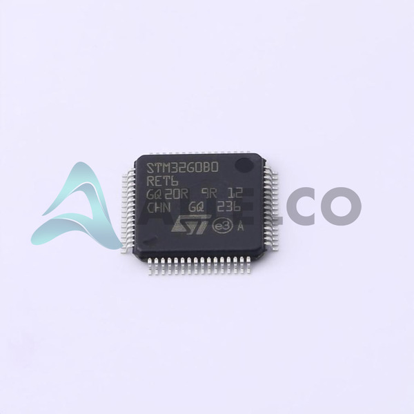
View All

Please refer to the English Version as our Official Version.Return

Europe
France(Français) Germany(Deutsch) Italy(Italia) Russian(русский) Poland(polski) Czech(Čeština) Luxembourg(Lëtzebuergesch) Netherlands(Nederland) Iceland(íslenska) Hungarian(Magyarország) Spain(español) Portugal(Português) Turkey(Türk dili) Bulgaria(Български език) Ukraine(Україна) Greece(Ελλάδα) Israel(עִבְרִית) Sweden(Svenska) Finland(Svenska) Finland(Suomi) Romania(românesc) Moldova(românesc) Slovakia(Slovenská) Denmark(Dansk) Slovenia(Slovenija) Slovenia(Hrvatska) Croatia(Hrvatska) Serbia(Hrvatska) Montenegro(Hrvatska) Bosnia and Herzegovina(Hrvatska) Lithuania(lietuvių) Spain(Português) Switzerland(Deutsch) United Kingdom(English)
Asia/Pacific
Japan(日本語) Korea(한국의) Thailand(ภาษาไทย) Malaysia(Melayu) Singapore(Melayu) Vietnam(Tiếng Việt) Philippines(Pilipino)
Africa, India and Middle East
United Arab Emirates(العربية) Iran(فارسی) Tajikistan(فارسی) India(हिंदी) Madagascar(malaɡasʲ)
South America / Oceania
New Zealand(Maori) Brazil(Português) Angola(Português) Mozambique(Português)
North America
United States(English) Canada(English) Haiti(Ayiti) Mexico(español)
HomeProductsIntegrated Circuits (ICs)Embedded - MicrocontrollersSTM32G0B0RET6
STM32G0B0RET6 Image
Image may be representation.
See specifications for product details.
EXPRESS OPTION
Payment method

STM32G0B0RET6 - STMicroelectronics

Manufacturer Part Number
STM32G0B0RET6
Manufacturer
STMicroelectronics
Allelco Part Number
32D-STM32G0B0RET6
Warranty
1 Year Allelco Warranty - Find out more
Stock Status:
18,454 pcs available, New & Original
Parts Description
IC MCU 32BIT 512KB FLASH 64LQFP
Package
64-LQFP (10x10)
Data sheet
STM32G0B0RET6.pdf
RoHs Status
ROHS3 Compliant
Our certification
In stock: 18454
  • Unit Price: $1.751
  • Subtotal: $0.00

Want a better price?
Add to Cart and Submit RFQ now, we'll contact you immediately.

Quantity Unit Price Ext. Price
1+ $1.751 $1.75
10+ $1.516 $15.16
30+ $1.369 $41.07
100+ $1.162 $116.20
500+ $1.094 $547.00
1000+ $1.064 $1,064.00
The above prices does not include taxes and freight rates, which will be calculated on the order pages.

Specifications

STM32G0B0RET6 Tech Specifications
STMicroelectronics - STM32G0B0RET6 technical specifications, attributes, parameters and parts with similar specifications to STMicroelectronics - STM32G0B0RET6

Product Attribute Attribute Value
Manufacturer STMicroelectronics
Voltage - Supply (Vcc/Vdd) 2V ~ 3.6V
Supplier Device Package 64-LQFP (10x10)
Speed 64MHz
Series STM32G0
RAM Size 144K x 8
Program Memory Type FLASH
Program Memory Size 512KB (512K x 8)
Peripherals Brown-out Detect/Reset, DMA, I²S, POR, PWM, WDT
Package / Case 64-LQFP
Package Tray
Product Attribute Attribute Value
Oscillator Type External, Internal
Operating Temperature -40°C ~ 85°C (TA)
Number of I/O 59
Mounting Type Surface Mount
EEPROM Size -
Data Converters A/D 19x12b SAR
Core Size 32-Bit Single-Core
Core Processor ARM® Cortex®-M0+
Connectivity HDMI-CEC, I²C, IrDA, LINbus, SPI, UART/USART, USB
Base Product Number STM32G0B0

Environmental & Export Classifications

ATTRIBUTE DESCRIPTION
RoHs Status ROHS3 Compliant
Moisture Sensitivity Level (MSL) 3 (168 Hours)
REACH Status REACH Unaffected
ECCN 3A991A2
HTSUS 8542.31.0001

Parts Introduction

STM32G0B0RET6 Image
STM32G0B0RET6 (1)

Manufacturer Part Number

STM32G0B0RET6

Manufacturer

STMicroelectronics

Introduction

High-performance STM32G0B0 32-Bit ARM Cortex-M0+ Microcontroller
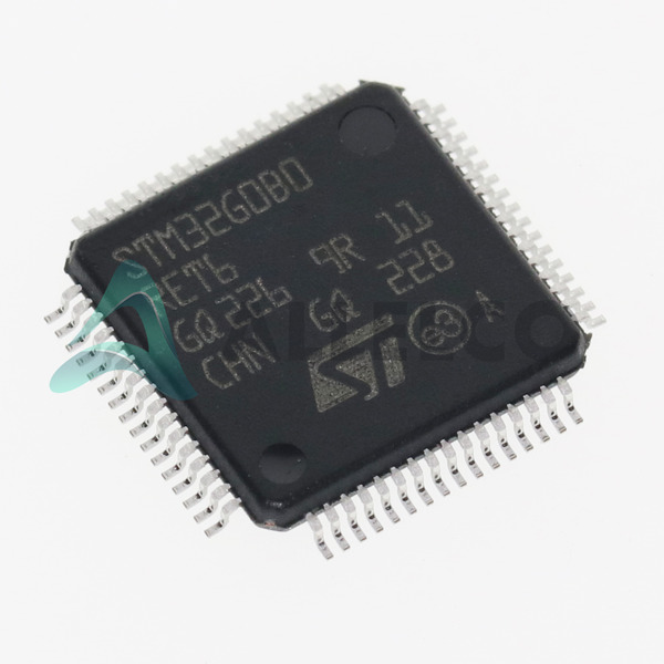
STM32G0B0RET6 Image
STM32G0B0RET6 (2)

Product Features and Performance

ARM Cortex-M0+ Core at 64MHz

High Integration with Advanced Peripherals

Energy-efficient Operation

Flash Memory of 512KB

RAM of 144K

Comprehensive I/O Support with 59 GPIOs

Enhanced Connectivity Options

Product Advantages

Low-power Consumption for Energy-sensitive Applications

STM32CubeMX Support for Easy Configuration

Large Ecosystem of Tools and Software

Robust Peripheral Set for Versatile Use

Key Technical Parameters

ARM Cortex-M0+ at 64MHz

512KB Flash Memory

144K RAM

59 I/O Ports

A/D Converters: 19x12b SAR

Quality and Safety Features

Brown-out Detect/Reset

Programmable Voltage Detector

Watchdog Timer

STM32G0B0RET6 Image
STM32G0B0RET6 (3)

Compatibility

Works with STM32G0 Series Ecosystem

Extensive Development Tools

Integrated with STM32Cube

Application Areas

Industrial Controls

Consumer Electronics

Automotive Systems

Internet of Things Devices

Product Lifecycle

Current Status: Active

Continuing Long-term Support

Several Key Reasons to Choose This Product

Optimized for Cost-sensitive Applications

Extended Temperature Range for Harsh Environments

Advanced Peripherals Enabling Complex Functionality

Scalability Within STM32G0 Series

Active Community and Manufacturer Support

Frequently Asked Questions(FAQ)

How does the STM32G0B0RET6 compare to other STM32G0 series microcontrollers in terms of memory capacity and peripheral integration for low-power embedded applications?
The STM32G0B0RET6 offers 512KB of flash memory and 144KB of RAM, making it one of the higher-capacity variants within the STM32G0 family. This positions it well-suited for applications requiring substantial firmware storage without transitioning to more power-hungry or expensive Cortex-M33-based devices. While lower-density G0 variants such as the STM32G070RB offer only 128KB flash, the B0 series maintains a balance between code space and cost for mid-complexity designs. The integrated peripherals—including USB 2.0 full-speed, LINbus, IrDA, and up to 19x12-bit ADCs—are consistently available across the G0 line, but the larger package and higher pin count of the LQFP-64 enable richer I/O mapping. Designers selecting this part should consider whether the additional memory justifies the marginal increase in bill-of-materials cost for projects where 256KB would suffice.
What is the impact of the STM32G0B0RET6’s voltage range on system-level power design when interfacing with sensors operating at 1.8V logic levels?
The STM32G0B0RET6 operates over a supply range of 2.0V to 3.6V, which means it can natively interface with 1.8V sensor systems through its built-in 5V-tolerant inputs and Schmitt-triggered GPIOs, provided that VDD remains above 2.0V. This eliminates the need for external level-shifting circuitry in many cases, reducing component count and board complexity. However, if the system must operate from a single 1.8V rail (e.g., powered by a battery), a direct connection may violate minimum VDD requirements. In such scenarios, an LDO stepping up to 2.0V or higher is necessary, introducing efficiency trade-offs. The microcontroller’s internal pull-up/pull-down resistors are active regardless of VDD as long as it exceeds the minimum threshold, aiding signal integrity during brown-out conditions.
Can the STM32G0B0RET6 reliably drive capacitive touch sensors in industrial environments with temperature variations between -40°C and +85°C?
Yes, the STM32G0B0RET6 includes hardware support for capacitive sensing via its advanced analog peripherals and timer resources, though it lacks dedicated capacitive touch controllers found in some STM32 families like the G4 or F7. Instead, designers implement software-based charge-transfer methods using general-purpose timers and GPIO pins. Within the specified operating temperature range (-40°C to 85°C), the internal oscillator accuracy degrades slightly compared to room temperature, potentially affecting timing precision in charge-transfer cycles. To compensate, calibration routines should be implemented at boot and periodically during operation. Additionally, the 12-bit SAR ADC provides sufficient resolution for reading baseline capacitance changes. Careful layout and shielding are essential to minimize noise, especially in electrically noisy industrial settings.
How does the STM32G0B0RET6 handle USB enumeration when used in battery-powered consumer electronics with variable input voltages?
The STM32G0B0RET6 integrates a full-speed USB 2.0 transceiver with embedded pull-up resistors configurable via software, supporting standard USB device mode operation. During enumeration, the USB PHY requires stable 3.3V supply; therefore, the MCU’s internal voltage regulator must remain active throughout the session. Since the device supports down to 2.0V VDD, a buck-boost converter or LDO is typically employed to maintain clean 3.3V for the USB block. Brown-out detection at user-programmable thresholds (down to ~1.85V) helps prevent erratic behavior during voltage dips, but frequent resets during discharge could disrupt enumeration. Designers should ensure adequate decoupling near the VBUS and VDD pins and consider adding a small capacitor on the internal regulator output if transient response is suboptimal.
What considerations apply when replacing the STM32G0B0RET6 with another STM32G0 variant in a legacy PCB footprint?
The STM32G0B0RET6 uses a 64-pin LQFP (10x10mm) package, which is compatible with standard footprints across the entire STM32G0 series. However, pin compatibility varies by subfamily—for example, the STM32G071RB uses the same package but fewer I/O lines. Replacing the part requires verifying that all required peripherals map correctly to available pins, particularly if USB D+/D−, NRST, or clock sources occupy non-overlapping assignments. Flash size differences also affect interrupt vector table placement; relocating it to RAM becomes necessary if migrating to a smaller-flash variant. Furthermore, the B0 series includes specific features like increased SRAM and dual-bank flash not present in earlier G0 releases, so software assumptions about memory layout must be audited. Always re-run configuration tools like STM32CubeMX post-migration to validate clock trees and peripheral mappings.
Is the STM32G0B0RET6 suitable for motor control applications requiring PWM generation at high frequencies?
The STM32G0B0RET6 includes advanced-control timers capable of generating center-aligned or edge-aligned PWM signals with dead-time insertion, making it viable for basic brushed DC motor control and stepper drivers. These timers support frequencies up to several hundred kHz, depending on counter resolution and prescaler settings. At 64MHz system clock, a 16-bit timer can achieve approximately 1kHz resolution, enabling fine duty-cycle granularity even at high switching rates. However, for three-phase PMSM or BLDC motors requiring field-oriented control (FOC), the lack of dedicated FOC hardware blocks limits performance compared to STM32G4 or STM32H7 devices. In such cases, software FOC implementations consume significant CPU cycles, potentially pushing the 64MHz Cortex-M0+ beyond sustainable utilization unless carefully optimized with assembly routines. For simpler unipolar steppers or gear motors, however, the MCU performs adequately with moderate current ratings.
How does the STM32G0B0RET6’s internal oscillator compare to an external crystal in terms of long-term stability for time-critical communication protocols?
The STM32G0B0RET6 incorporates a calibrated 16MHz internal HSI oscillator with ±1% accuracy over temperature and voltage, suitable for most UART, SPI, and I2C applications. However, for precise baud rate generation or synchronous protocols like SmartCard (ISO 7816), where timing tolerances are strict, an external 4–32MHz crystal provides superior stability—typically ±10 ppm or better. The internal RC oscillator drifts significantly under varying load capacitance or ambient conditions, leading to accumulated errors over extended periods. When using USB, the internal HSI cannot serve as the USB clock source; instead, either an external 48MHz clock derived from a crystal or PLL-synthesized 48MHz from HSE is mandatory. Thus, mission-critical timing applications benefit from HSE/HSE16M16V external oscillators despite added board real estate and component cost.
What risks arise when operating the STM32G0B0RET6 near its maximum junction temperature under continuous computational load?
The STM32G0B0RET6 is rated for commercial operation up to 85°C ambient (TA), with thermal resistance (junction-to-ambient) around 45°C/W in typical PCB layouts. Under sustained full-load execution—such as running FFT algorithms, managing multiple UART streams, or processing ADC data in real time—internal power dissipation may exceed 200mW, causing junction temperature (TJ) to rise above TA by 80–100°C. Prolonged exposure near TJmax (~150°C) accelerates electromigration and reduces mean time between failures. Designers must ensure adequate airflow, copper pours on adjacent layers, or derate clock speeds during peak loads. Monitoring the Temperature Sensor peripheral (if available) or implementing throttling logic based on internal ADC readings can mitigate risk. Note that brown-out reset and WDT functions remain functional regardless of temperature, preserving system recovery mechanisms.
Can the STM32G0B0RET6 support secure boot functionality without additional hardware security modules?
The STM32G0B0RET6 does not include TrustZone technology or hardware cryptographic accelerators like AES-CCM found in higher-end G0 variants (e.g., STM32G071xx). Therefore, it cannot perform onboard secure boot using tamper-resistant key storage. However, basic integrity checks can be implemented via software using SHA-256 hashing libraries, with keys stored in read-protected flash sectors. Secure boot would require external flash with write-protection capabilities and possibly a separate secure element for key management. Without hardware isolation, any compromise of the application code could expose secrets. For low-to-mid security requirements—such as preventing firmware modification in unattended devices—this approach may suffice, but it lacks the robustness of platforms with built-in secure provisioning and anti-cloning features.
What trade-offs exist between using DMA versus polling for UART reception on the STM32G0B0RET6 in a multi-channel sensor network?
Polling UART receive interrupts on the STM32G0B0RET6 consumes predictable CPU cycles per byte, which may suffice for low-data-rate sensors (<115.2 kbps). However, in multi-sensor networks where multiple USARTs stream data simultaneously, polling leads to latency spikes and missed characters during burst traffic. Enabling DMA channels linked to each USART frees the Cortex-M0+ core to handle protocol parsing or sensor fusion while background transfers complete automatically. The STM32G0B0RET6 supports up to 12 DMA channels, allowing concurrent handling of SPI, I2C, and UART traffic. The trade-off is increased memory footprint due to buffer allocation and potential complexity in managing circular buffers. Given the limited RAM (144KB), buffers must be sized conservatively, and double-buffering strategies should be avoided unless memory permits. Overall, DMA improves responsiveness and reduces worst-case latency at the expense of modest development overhead.
How does the STM32G0B0RET6 manage power consumption during deep sleep modes when maintaining RTC and backup register contents?
The STM32G0B0RET6 supports multiple low-power modes including Sleep, Stop, and Standby. In Stop mode, the CPU halts but retains SRAM and registers via the internal voltage regulator, drawing typically 50µA at 3.3V. With RTC enabled and LSE (low-speed external crystal) running, total current drops below 3µA. The Standby mode cuts off most power domains except backup domain, reducing consumption to <2µA. Backup registers remain intact across both modes, preserving critical state information. Transition times from Stop to Run mode are under 2µs, enabling fast wake-up for event-driven applications. However, restoring full functionality requires careful reinitialization of clocks and peripherals. Designers should disable unused peripherals before entering low-power states and leverage the Ultra Low-Power Timer (ULPTIM) for periodic wake triggers without waking the main CPU unnecessarily.
Are there known limitations when using the STM32G0B0RET6’s USB interface in self-powered configurations without external ESD protection?
The STM32G0B0RET6 includes basic ESD protection on USB D+/D− pins (±8kV HBM per JEDEC), but this is insufficient for industrial or automotive environments with high electrostatic transients. Without external TVS diodes (e.g., SMBJ6.5CA), repeated ESD events can degrade internal ESD structures over time, eventually leading to functional failure. Additionally, self-powered designs must ensure that VBUS is properly monitored and disconnected when absent to avoid back-powering the MCU. The internal pull-up resistor on D+ must be set correctly to signal device presence. While compliant with USB 2.0 specification, robust deployment in harsh environments demands supplemental protection circuits near the connector, especially if hot-plugging is expected. Failure to do so increases risk of field returns due to intermittent connectivity or reset loops.
What factors influence flash memory endurance when frequently updating non-volatile parameters on the STM32G0B0RET6?
The STM32G0B0RET6’s flash memory has a typical endurance rating of 10,000 program/erase cycles per sector, consistent with modern STMicroelectronics processes. Frequent writes to the same address accelerate wear, potentially shortening device lifespan in logging-heavy applications. To extend longevity, implement wear-leveling algorithms that distribute updates across multiple sectors. Alternatively, store only delta changes in RAM and write consolidated values periodically. The MCU supports byte-level programming within pages (usually 2KB), minimizing erase operations. Note that flash erase occurs at the page level, so partial-page writes require careful alignment. Using the Option Bytes or user-defined flash areas for configuration avoids corrupting critical code regions. Monitoring cumulative erase counts via counters in RAM or EEPROM (if available) helps predict end-of-life. For mission-critical systems, consider sparing a dedicated flash sector solely for runtime statistics.
How does the STM32G0B0RET6’s LINbus implementation compare to dedicated LIN transceivers in terms of noise immunity and bus fault tolerance?
The STM32G0B0RET6 includes a LIN 2.2-compliant physical layer interface capable of driving LIN signals directly, eliminating the need for external transceivers like TJA1020. This integration reduces BOM count and simplifies routing. However, standalone LIN transceivers often provide higher slew rate control, better common-mode voltage handling, and enhanced EMC performance due to optimized output stages. In electrically noisy environments with long stubbed buses or mixed-voltage nodes, external transceivers improve fault tolerance by isolating ground loops and limiting current surges. The MCU’s internal driver may struggle with large cable lengths (>10 meters) or high node counts without additional termination. Moreover, diagnostic features like short-circuit detection are typically absent, increasing debugging difficulty. For simple node counts (<8) and short runs (<4 meters), the onboard LIN interface suffices, but complex networks benefit from proven external solutions.
What precautions are necessary when bootloading firmware onto the STM32G0B0RET6 via USART without erasing the entire flash?
Bootloading over USART requires the bootloader to reside in System Memory (ROM), accessible after setting the nBOOT0 pin high and releasing NRST. Firmware updates must respect flash page boundaries; attempting to write across page seams without erasing causes corruption. The STM32G0B0RET6 organizes flash into pages of 2KB (varies slightly by density), so partial-page writes necessitate prior erase. Implement a CRC32 check on received images and verify against expected value before committing to flash. Also, disable interrupts during flash operations to prevent timing violations. If the update fails midway, the device may become unresponsive until reflashed via SWD. To recover, ensure BOOT0/BOOT1 pins are configured for ROM bootloader entry upon next reset. Never overwrite the bootloader region itself unless updating to a newer version from ST.
How does the STM32G0B0RET6’s I2S peripheral support multi-master audio streaming without glitches when sharing the bus with other masters?
The STM32G0B0RET6 features an I2S interface compatible with standard SAI (Serial Audio Interface) protocols, capable of acting as master or slave. In multi-master scenarios, contention arises when multiple devices attempt to drive SCK/WS simultaneously. The STM32G0B0RET6 lacks built-in arbitration logic, so collision detection and resolution must be managed externally or via software coordination. One common strategy involves using a centralized frame sync generator or configuring one master as primary clock source. Alternatively, employ Mute Mode or disable TX/RX during conflict windows. Due to the absence of hardware flow control for I2S, timing jitter can accumulate, leading to audio artifacts. For reliable multi-drop audio, consider daisy-chaining slaves or using dedicated audio codecs with internal FIFO buffering to absorb clock mismatches. The limited RAM (144KB) restricts large audio buffers, favoring compressed formats or lower sample rates.
What design constraints apply when integrating the STM32G0B0RET6 with external memory (e.g., SPI NOR flash) for code execution?
The STM32G0B0RET6 does not support XIP (execute-in-place) from external memory via standard interfaces. Code must be executed exclusively from internal flash. However, external SPI NOR flash can serve as secondary storage for logs, configurations, or large datasets. To expand persistent storage, use QSPI (Quad-SPI) if available—though the G0B0RET6 lacks native QSPI hardware. Instead, bit-banging SPI with DMA can transfer data blocks into RAM for processing. For faster access, partition internal flash into code and data sections, loading infrequently used functions dynamically from external flash into RAM. This approach trades memory for speed but complicates linking and debugging. Always ensure that external memory accesses do not starve the CPU during critical real-time tasks, given the 64MHz core bandwidth constraints.
How does the STM32G0B0RET6’s Moisture Sensitivity Level (MSL 3) affect manufacturing handling and shelf life in high-volume production?
As an MSL 3 component (168-hour limit after opening), the STM32G0B0RET6 must be stored in dry packaging (humidity <10%) prior to assembly. Once opened, exposure to ambient humidity begins degrading lead-free solder joint reliability due to moisture absorption. Manufacturers typically enforce a 168-hour window before reflow soldering; exceeding this may require bake-out cycles to remove trapped moisture, increasing costs. High-volume producers use humidity-controlled cabinets and automated tape-and-reel feeding to minimize open time. For prototypes or low-volume builds, operators must track date codes and adhere to IPC/JEDEC J-STD-033 guidelines. Failure to comply risks pop-corning during reflow, leading to cracked packages or latent defects. Always follow distributor-specific handling instructions and maintain proper documentation for traceability.

Parts with Similar Specifications

The three parts on the right have similar specifications to STMicroelectronics STM32G0B0RET6

Product Attribute STM32G0B0RET6TR STM32G0B0CET6TR STM32G0B0CET6 STM32G0B0KET6
Part Number STM32G0B0RET6TR STM32G0B0CET6TR STM32G0B0CET6 STM32G0B0KET6
Manufacturer STMicroelectronics STMicroelectronics STMicroelectronics STMicroelectronics
Peripherals - - - -
Package / Case - 196-LFBGA 16-DIP (0.300', 7.62mm) 64-VFQFN Exposed Pad
RAM Size - - - -
Operating Temperature - -40°C ~ 85°C 0°C ~ 70°C -40°C ~ 85°C
Voltage - Supply (Vcc/Vdd) - - - -
Package - Tape & Reel (TR) Tube Tape & Reel (TR)
Base Product Number - DAC34H84 MAX500 ADS62P42
EEPROM Size - - - -
Series - - - -
Program Memory Size - - - -
Core Size - - - -
Supplier Device Package - 196-NFBGA (12x12) 16-PDIP 64-VQFN (9x9)
Number of I/O - - - -
Mounting Type - Surface Mount Through Hole Surface Mount
Connectivity - - - -
Data Converters - - - -
Core Processor - - - -
Oscillator Type - - - -
Program Memory Type - - - -
Speed - - - -

STM32G0B0RET6 Datasheet PDF

Download STM32G0B0RET6 pdf datasheets and STMicroelectronics documentation for STM32G0B0RET6 - STMicroelectronics.

Datasheets
STM32G0B0(K,C,R,V)E.pdf
PCN Design/Specification
Datasheets enhancement 01/Sep/2021.pdf STM32G0x 28/Jun/2022.pdf
Errata
STM32G0B0(K,C,R,V)E.pdf

Customer Reviews

Evaluation: 10 Articles

  • Dani***alkerTech
    Jun 1, 2026

    Product works, but setup took more effort than expected. Once configured the MCU ran reliably, although documentation support felt older compared with newer platforms. Fine for maintenance projects.

  • Yuki***aka88
    May 26, 2026

    信号通信プロジェクトでこのRS-485トランシーバーを使用しました。設置は簡単で、長距離ケーブルでも通信は安定していました。消費電力も、以前使用していたものより低くなっています。

  • Stev***aker
    May 20, 2026

    Solid diode for power rectification. Works well in switching circuits.

  • Bran***Lewis
    May 11, 2026

    Compact FPGA with good performance. Suitable for basic signal processing tasks.

  • Oliv***arris
    May 7, 2026

    Reliable I/O expander. Works well in embedded control applications.

  • Jess***Jones
    Apr 17, 2026

    It offers good value for the price, and the specifications match the description. I’ve been using it for two days with no issues, and I’ll definitely buy it again if I need it in the future.

  • Mich***Smith
    Apr 17, 2026

    Shipping was on time, the component pins are neatly aligned, and I tested 10 of them with a multimeter—all readings were within the specified range. Highly recommended.

  • Aman***arris
    Apr 3, 2026

    It was great—the entire process, from placing the order to receiving the package, went very smoothly. The components were consistent, the price was fair, and I had a very pleasant shopping experience.

  • Mike***nch
    Apr 3, 2026

    Better than expected! The resistance and capacitance readings were spot-on, and it passed the test on the first try. The service was reliable, and the packaging was thoughtful—I highly recommend it.

  • Daic***K.
    Mar 23, 2026

    Very good. No issue after long time testing.

Write a Review

Your Email address will not be published.

Shipment

Delivery Time

In-stock items can be shipped within 24 hours. Some parts will be arranged for delivery within 1-2 days from the date all items arrive at our warehouse. And Allelco ships order once a day at about 17:00, except Sunday. Once the goods are shipped, the estimated delivery time depends on the shipping methods and Delivery destination. The table below shows are the logistic time for some common countries.

Delivery Cost

  1. Use your express account for shipment if you have one.
  2. Use our account for the shipment. Refer to the table below for the approximate charges.
(Different time frame / countries / package size has different price.)

Delivery Method

  1. Global Common Shipment by DHL / UPS / FedEx / TNT / EMS / SF we support.
  2. Others more shipping ways, please get in touch with your customer manager.

Common Countries Logistic Time Reference
Region Country Logistic Time(Day)
America United States 5
Brazil 7
Europe Germany 5
United Kingdom 4
Italy 5
Oceania Australia 6
New Zealand 5
Asia India 4
Japan 4
Middle East Israel 6
DHL & FedEx Shipment Charges Reference
Shipment charges(KG) Reference DHL(USD$)
0.00kg-1.00kg USD$30.00 - USD$60.00
1.00kg-2.00kg USD$40.00 - USD$80.00
2.00kg-3.00kg USD$50.00 - USD$100.00
Note:
The above table is for reference only. There may have some data bias for the uncontrollable factors.
Contact us if you have any questions.
  • QC (Quality Warranty)
  • Payment Support
  • Packaging
  • Certifications & Memberships

QC (Quality Warranty)

Allelco is committed to exceeding customer expectations through customer service excellence, order accuracy, and on-time delivery.
This is achieved through our commitment to the continual improvement of our processes, services, and products.


Strict quality inspection builds a solid foundation for electronic component quality.
  1. Visual inspection
  2. Performance testing and reliability verification
  3. Standardized full-process testing
  4. Precise control of every parameter
We eliminate defective components and ensure the stable operation of electronic devices through professional quality standards.

Payment Support

The payment method can be chosen from the methods shown below: Wire Transfer (T/T, Bank Transfer), Western Union, Credit card, PayPal.
  • HKBea
  • Paypal
  • MasterCard
  • Western-Union
  • VISA
Stable Delivery, Sincere Partnership — Your Faithful Supply Chain Partner
  • Efficient Supply Management
  • Cost-Saving Procurement
  • Fast Sourcing & Delivery
Contact us if you have any questions.

Packaging

Electrostatic Discharge Protection and Handling

All electrostatic-sensitive components are handled in accordance with electrostatic discharge control procedures. The products are hermetically sealed in anti-static safe packaging to prevent electrostatic damage. Appropriate labeling is also applied for identification and traceability. This ensures product integrity during storage, handling and transportation.


ESD

Certifications & Memberships

Third-party certified, strict quality control. Our certification
  • ISO 9001: 2015
  • ISO 13485: 2016
  • ISO 14001: 2015
  • ISO 28000: 2007
  • ISO 45001: 2018
  • GB/T 27922-2011
  • SMTA
  • IPC
  • ESD
  • PSMA
STM32G0B0RET6 Image

STM32G0B0RET6

STMicroelectronics
32D-STM32G0B0RET6

Want a better price? Add to Cart and Submit RFQ now, we'll contact you immediately.

0 RFQ
Shopping cart (0 Items)
It is empty.
Compare List (0 Items)
It is empty.
Feedback

Your feedback matters! At Allelco, we value the user experience and strive to improve it constantly.
Please share your comments with us via our feedback form, and we'll respond promptly.
Thank you for choosing Allelco.

Subject
E-mail
Comments
Captcha
Drag or click to upload file
Upload File
types: .xls, .xlsx, .doc, .docx, .jpg, .png and .pdf.
Max file size: 10MB