
 STM32L471ZGT6STMicroelectronicsIC MCU 32BIT 1MB FLASH 144LQFP
 STM32L471ZGJ6STMicroelectronicsIC MCU 32BIT 1MB FLASH 144UFBGA
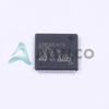 STM32L475VCT6STMicroelectronicsIC MCU 32BIT 256KB FLASH 100LQFP
 STM32L475RCT6STMicroelectronics
- Dani***alkerTech
- Jun 1, 2026


Image may be representation.
See specifications for product details.
See specifications for product details.
- EXPRESS OPTION
- Payment method
STM32L475RCT7 - STMicroelectronics
- Manufacturer Part Number
- STM32L475RCT7
- Manufacturer
- STMicroelectronics
- Allelco Part Number
- 98D-STM32L475RCT7
- Warranty
- 1 Year Allelco Warranty - Find out more
- Stock Status:
- 42,350 pcs available, New & Original
- Parts Description
- IC MCU 32BIT 256KB FLASH 64LQFP
- Package
- 64-LQFP (10x10)
- Data sheet
-
STM32L475RCT7.pdf
PCN Packaging
2.73KHz.pdfPCN Design/Specification
STM32L4y Datasheet Chg 7/Feb/2020.pdf Mult Dev Material Chgs 28/Feb/2023.pdfPCN Assembly/Origin
STM8/STM32 10/Mar/2020.pdfHTML Datasheet
STM32L475xx Datasheet.pdf
- RoHs Status
- ROHS3 Compliant
- Our certification
- In stock: 42350
- Unit Price: $5.813
- Subtotal: $0.00
Want a better price?
Add to Cart and Submit RFQ now, we'll contact you immediately.
| Quantity | Unit Price | Ext. Price |
|---|---|---|
| 1+ | $5.813 | $5.81 |
The above prices does not include taxes and freight rates, which will be calculated on the order pages.


