View All

Please refer to the English Version as our Official Version.Return

Europe
France(Français) Germany(Deutsch) Italy(Italia) Russian(русский) Poland(polski) Czech(Čeština) Luxembourg(Lëtzebuergesch) Netherlands(Nederland) Iceland(íslenska) Hungarian(Magyarország) Spain(español) Portugal(Português) Turkey(Türk dili) Bulgaria(Български език) Ukraine(Україна) Greece(Ελλάδα) Israel(עִבְרִית) Sweden(Svenska) Finland(Svenska) Finland(Suomi) Romania(românesc) Moldova(românesc) Slovakia(Slovenská) Denmark(Dansk) Slovenia(Slovenija) Slovenia(Hrvatska) Croatia(Hrvatska) Serbia(Hrvatska) Montenegro(Hrvatska) Bosnia and Herzegovina(Hrvatska) Lithuania(lietuvių) Spain(Português) Switzerland(Deutsch) United Kingdom(English)
Asia/Pacific
Japan(日本語) Korea(한국의) Thailand(ภาษาไทย) Malaysia(Melayu) Singapore(Melayu) Vietnam(Tiếng Việt) Philippines(Pilipino)
Africa, India and Middle East
United Arab Emirates(العربية) Iran(فارسی) Tajikistan(فارسی) India(हिंदी) Madagascar(malaɡasʲ)
South America / Oceania
New Zealand(Maori) Brazil(Português) Angola(Português) Mozambique(Português)
North America
United States(English) Canada(English) Haiti(Ayiti) Mexico(español)
HomeProductsIntegrated Circuits (ICs)Embedded - FPGAs (Field Programmable Gate Array)LCMXO2-7000HC-4TG144I
LCMXO2-7000HC-4TG144I Image
Image may be representation.
See specifications for product details.
EXPRESS OPTION
Payment method

LCMXO2-7000HC-4TG144I - Lattice Semiconductor Corporation

Manufacturer Part Number
LCMXO2-7000HC-4TG144I
Manufacturer
Lattice Semiconductor
Allelco Part Number
32D-LCMXO2-7000HC-4TG144I
Warranty
1 Year Allelco Warranty - Find out more
Stock Status:
2,364 pcs available, New & Original
Parts Description
IC FPGA 114 I/O 144TQFP
Package
144-TQFP (20x20)
Data sheet
LCMXO2-7000HC-4.pdf
RoHs Status
ROHS3 Compliant
Our certification
In stock: 2364
  • Unit Price: $21.58
  • Subtotal: $0.00

Want a better price?
Add to Cart and Submit RFQ now, we'll contact you immediately.

Quantity Unit Price Ext. Price
1+ $21.58 $21.58
30+ $20.61 $618.30
The above prices does not include taxes and freight rates, which will be calculated on the order pages.

Specifications

LCMXO2-7000HC-4TG144I Tech Specifications
Lattice Semiconductor Corporation - LCMXO2-7000HC-4TG144I technical specifications, attributes, parameters and parts with similar specifications to Lattice Semiconductor Corporation - LCMXO2-7000HC-4TG144I

Product Attribute Attribute Value
Manufacturer Lattice Semiconductor
Voltage - Supply 2.375V ~ 3.465V
Total RAM Bits 245760
Supplier Device Package 144-TQFP (20x20)
Series MachXO2
Package / Case 144-LQFP
Package Tray
Product Attribute Attribute Value
Operating Temperature -40°C ~ 100°C (TJ)
Number of Logic Elements/Cells 6864
Number of LABs/CLBs 858
Number of I/O 114
Mounting Type Surface Mount
Base Product Number LCMXO2-7000

Environmental & Export Classifications

ATTRIBUTE DESCRIPTION
RoHs Status ROHS3 Compliant
Moisture Sensitivity Level (MSL) 3 (168 Hours)
REACH Status REACH Unaffected
ECCN EAR99
HTSUS 8542.39.0001

Parts Introduction

LCMXO2-7000HC-4TG144I Image
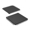
LCMXO2-7000HC-4TG144I (1)

Manufacturer Part Number

LCMXO2-7000HC-4TG144I

Manufacturer

Lattice Semiconductor

Introduction

Lattice MachXO2 series FPGA designed for low power, small footprint, and cost-sensitive applications

Product Features and Performance

858 Look-Up Tables (LUTs) for logic functions

6864 logic cells for design flexibility

245760 total RAM bits for data storage

114 available general-purpose I/O pins

Versatile power supply voltage range from 2.375V to 3.465V

Surface mount 144-LQFP package for compact PCB design

Extended operating temperature range of -40°C to 100°C suitable for industrial applications

Product Advantages

Low power consumption ideal for power-sensitive devices

Small footprint suited for space-constrained applications

Robust temperature range for use in harsh environments

Reconfigurable logic cells support complex logic designs

Non-volatile configuration memory enhances device security

Key Technical Parameters

Number of LABs/CLBs: 858

Number of Logic Elements/Cells: 6864

Total RAM Bits: 245760

Number of I/O: 114

Voltage Supply Range: 2.375V to 3.465V

Mounting Type: Surface Mount

Operating Temperature: -40°C to 100°C (TJ)

Package/Case: 144-LQFP

Supplier Device Package: 144-TQFP (20x20)

Quality and Safety Features

Strict adherence to industry quality and safety standards

Robust construction for operation in industrial temperature ranges

Compatibility

Compatible with Lattice programming and development tools

Broad interoperability with various standard interfaces

Application Areas

Industrial automation

Consumer electronics

Telecommunications infrastructure

Automotive electronics

Defense and aerospace systems

Product Lifecycle

Product status is active

Not approaching discontinuation

Future upgrade paths are available through the MachXO2 product family

Several Key Reasons to Choose This Product

High-density logic cell count offering design versatility

Integrated memory for efficient data handling

Multiple I/O options for flexible connectivity

Low power consumption to extend battery life in portable devices

Robust performance across a wide temperature range for reliability in demanding applications

Lattice Semiconductor's commitment to long-term product availability and support

Frequently Asked Questions(FAQ)

How does the LCMXO2-7000HC-4TG144I handle power sequencing requirements during startup, and what design considerations are necessary to ensure reliable initialization?
The LCMXO2-7000HC-4TG144I requires that the core voltage (VCCINT) and I/O bank voltages (VCCIOx) be stable within the 2.375V to 3.465V range before configuration begins. While the device supports hot-swap and partial power sequencing, best practice dictates a monotonic rise of VCCINT prior to or simultaneously with VCCIO banks to prevent unintended I/O contention. A delay of at least 100 µs between power stabilization and asserting PROGRAMN is recommended to allow internal power-on reset circuits to settle. Designers should incorporate power supervisors with precise thresholds (±2% tolerance) to meet these timing margins, especially in multi-rail systems where brownout recovery could trigger unintended reconfiguration.
What is the effective usable logic capacity of the LCMXO2-7000HC-4TG144I when implementing a moderately complex state machine with embedded memory and I/O buffering?
With 6,864 logic elements and 245,760 bits of embedded block RAM, the LCMXO2-7000HC-4TG144I can typically support designs requiring up to 4,000–5,000 utilized LUTs while reserving sufficient resources for routing overhead, clock management, and I/O logic. For example, a dual-channel SPI controller with FIFOs and error-checking logic might consume approximately 1,200 LUTs and two EBR blocks (18 Kb total), leaving ample headroom for additional control logic. However, dense interconnect patterns or high-fanout nets can reduce effective utilization by 15–20% due to placement constraints, so floorplanning early in the design flow is advised.
How does the LCMXO2-7000HC-4TG144I compare to the LCMXO2-4000HE in terms of real-world performance for low-power industrial sensor interfaces?
The LCMXO2-7000HC-4TG144I offers approximately 70% more logic elements (6,864 vs. 4,100) and double the block RAM (245,760 vs. 122,880 bits) compared to the LCMXO2-4000HE, enabling more complex data preprocessing or protocol handling within a single device. In a typical 3.3V industrial sensor hub application sampling four analog channels via SPI ADCs, the LCMXO2-7000HC-4TG144I can implement real-time filtering and timestamping without external glue logic, whereas the LCMXO2-4000HE may require offloading to a microcontroller. Both devices share the same static power profile (~35 µW/MHz), but the larger device’s ability to consolidate functions reduces total system power by eliminating interface ICs.
What are the thermal implications of operating the LCMXO2-7000HC-4TG144I at maximum junction temperature in a sealed industrial enclosure?
At TJ = 100°C and ambient temperatures approaching 85°C, the LCMXO2-7000HC-4TG144I’s power dissipation must be carefully managed to avoid thermal runaway. In a typical 3.3V application with 60% logic utilization and 20 active I/Os switching at 10 MHz, dynamic power can reach ~180 mW. Combined with ~50 mW static power, this yields a total of ~230 mW. Given the 144-TQFP package’s θJA of ~35°C/W (on a 4-layer PCB), the resulting temperature rise is approximately 8°C above ambient. However, in sealed enclosures with limited airflow, localized heating from adjacent components can elevate effective ambient temperature, necessitating thermal vias under the package and copper pour isolation to maintain TJ within limits.
Can the LCMXO2-7000HC-4TG144I support DDR3 memory interfacing through soft IP, and what are the limiting factors?
The LCMXO2-7000HC-4TG144I lacks hardened memory controllers and high-speed transceivers, making native DDR3 support impractical. However, a soft-core DDR3 controller can be implemented using the available 6,864 logic elements and block RAM, though with significant trade-offs. Maximum achievable data rates are limited to ~800 Mbps (DDR3-800) due to the FPGA’s 1.2V VCCIO limitations and lack of calibrated delay-locked loops (DLLs) for precise DQS alignment. Additionally, the 114 I/Os constrain address/command bus width—practical implementations typically cap at 16-bit data widths. For applications requiring higher bandwidth or reliability, an external memory controller or migration to a higher-performance FPGA family is recommended.
How does the LCMXO2-7000HC-4TG144I’s configuration memory architecture impact firmware update strategies in field-deployed systems?
The LCMXO2-7000HC-4TG144I uses non-volatile flash-based configuration memory, retaining programming without external boot devices. This enables single-chip solutions but introduces considerations for in-field updates. The internal flash supports over 10,000 program/erase cycles, sufficient for most industrial lifecycles, but frequent reprogramming (e.g., daily updates) may necessitate wear-leveling algorithms in the host MCU’s firmware. Dual-boot support is not native; instead, designers must implement a soft-core state machine to manage fallback images stored in external SPI flash. Configuration time is ~10 ms from power-on, so fail-safe mechanisms should account for brief unavailability during updates.
What signal integrity challenges arise when routing high-speed SPI or UART interfaces on the LCMXO2-7000HC-4TG144I’s 144-TQFP package?
The 144-TQFP’s 0.5 mm pitch and lead inductance (~2–3 nH per pin) impose constraints on signal integrity for interfaces operating above 20 MHz. For SPI clocks exceeding 25 MHz, transmission line effects become significant, requiring controlled impedance routing (typically 50 Ω single-ended) and length matching within ±50 ps for data lines. Ground return paths must be maintained beneath high-speed traces to minimize crosstalk, especially given the limited number of dedicated GND pins (12 in this package). Additionally, simultaneous switching output (SSO) noise can couple into adjacent analog or clock signals; isolating high-drive I/O banks and using slew rate control (available in the LCMXO2-7000HC-4TG144I’s programmable I/O buffers) mitigates this risk.
How does the LCMXO2-7000HC-4TG144I’s MachXO2 architecture compare to Xilinx CoolRunner-II CPLDs for glue logic applications in legacy system upgrades?
The LCMXO2-7000HC-4TG144I provides significantly greater flexibility than CoolRunner-II devices, offering 6,864 logic elements versus ~500–1,000 in comparable CPLDs, along with embedded block RAM and hardened SPI flash. This enables implementation of complex state machines, protocol converters, or soft processors that would require multiple CoolRunner-II chips. However, for simple glue logic (e.g., address decoding or signal multiplexing), the CoolRunner-II’s instant-on capability and lower static power (~10 µA vs. ~50 µA in standby) may be preferable. The LCMXO2-7000HC-4TG144I excels in applications requiring future scalability or firmware-based reconfiguration, while CoolRunner-II remains viable for deterministic, low-latency combinatorial logic.
What precautions are necessary when designing the PCB layout for the LCMXO2-7000HC-4TG144I to meet MSL 3 handling requirements?
As an MSL 3 device, the LCMXO2-7000HC-4TG144I can withstand ambient storage for 168 hours before requiring baking if exposed to >30°C/60% RH conditions. To prevent moisture-induced delamination during reflow, PCBs must be baked at 125°C for 24 hours if the floor life is exceeded. During layout, ensure even thermal distribution under the package by using a symmetrical ground plane and thermal vias (8–12 vias of 0.3 mm diameter recommended) to avoid warpage. Stencil aperture design should limit solder paste volume to prevent voiding, and no-clean flux is preferred to reduce ionic contamination risks that could affect long-term reliability in humid environments.
Can the LCMXO2-7000HC-4TG144I be used in safety-critical applications requiring IEC 61508 compliance, and what documentation support is available?
While the LCMXO2-7000HC-4TG144I is not certified to IEC 61508, its deterministic timing, non-volatile configuration, and absence of dynamic reconfiguration make it suitable for use in SIL 1 or SIL 2 systems with proper architectural mitigations. Lattice provides reliability reports including FIT rates (<10 FIT at 55°C) and failure mode distribution data, which can support FMEDA development. Designers must implement external watchdog timers and periodic self-test routines, as the device lacks built-in BIST or redundancy features. For higher integrity levels, consider pairing with a certified microcontroller for cross-monitoring, leveraging the FPGA’s role as a peripheral controller rather than primary safety logic.

Parts with Similar Specifications

The three parts on the right have similar specifications to Lattice Semiconductor Corporation LCMXO2-7000HC-4TG144I

Product Attribute LCMXO2-7000HC-4TG144C LCMXO2-7000HC-4FG484I LCMXO2-7000HC-4FTG256I LCMXO2-7000HC-4FG484C
Part Number LCMXO2-7000HC-4TG144C LCMXO2-7000HC-4FG484I LCMXO2-7000HC-4FTG256I LCMXO2-7000HC-4FG484C
Manufacturer Lattice Semiconductor Corporation Lattice Semiconductor Corporation Lattice Semiconductor Corporation Lattice Semiconductor Corporation
Mounting Type - Surface Mount Through Hole Surface Mount
Package / Case - 196-LFBGA 16-DIP (0.300', 7.62mm) 64-VFQFN Exposed Pad
Operating Temperature - -40°C ~ 85°C 0°C ~ 70°C -40°C ~ 85°C
Number of LABs/CLBs - - - -
Total RAM Bits - - - -
Package - Tape & Reel (TR) Tube Tape & Reel (TR)
Voltage - Supply - - - -
Series - - - -
Number of I/O - - - -
Number of Logic Elements/Cells - - - -
Supplier Device Package - 196-NFBGA (12x12) 16-PDIP 64-VQFN (9x9)
Base Product Number - DAC34H84 MAX500 ADS62P42

LCMXO2-7000HC-4TG144I Datasheet PDF

Download LCMXO2-7000HC-4TG144I pdf datasheets and Lattice Semiconductor Corporation documentation for LCMXO2-7000HC-4TG144I - Lattice Semiconductor Corporation.

Datasheets
MachXO2 Family Datasheet.pdf
PCN Packaging
All Dev Pkg Mark Chg 12/Nov/2018.pdf
PCN Assembly/Origin
Alternate Qualified Test Site 30/Sep/2013.pdf
Manuals
Leaded Pkg PCB Layout Guide.pdf
PCN Design/Specification
MachXO2 Family Datasheet 30/Sep/2013.pdf QFP Dev Marking Chgs 28/Sep/2020.pdf

Customer Reviews

Evaluation: 10 Articles

  • Nath***rooks
    Jun 11, 2026

    Installed this power component in a converter board. Output remained stable under different load conditions and thermal performance was better than expected.

  • Dani***alkerTech
    Jun 1, 2026

    Product works, but setup took more effort than expected. Once configured the MCU ran reliably, although documentation support felt older compared with newer platforms. Fine for maintenance projects.

  • Yuki***aka88
    May 26, 2026

    信号通信プロジェクトでこのRS-485トランシーバーを使用しました。設置は簡単で、長距離ケーブルでも通信は安定していました。消費電力も、以前使用していたものより低くなっています。

  • Stev***aker
    May 20, 2026

    Solid diode for power rectification. Works well in switching circuits.

  • Bran***Lewis
    May 11, 2026

    Compact FPGA with good performance. Suitable for basic signal processing tasks.

  • Oliv***arris
    May 7, 2026

    Reliable I/O expander. Works well in embedded control applications.

  • Jess***Jones
    Apr 17, 2026

    It offers good value for the price, and the specifications match the description. I’ve been using it for two days with no issues, and I’ll definitely buy it again if I need it in the future.

  • Mich***Smith
    Apr 17, 2026

    Shipping was on time, the component pins are neatly aligned, and I tested 10 of them with a multimeter—all readings were within the specified range. Highly recommended.

  • Aman***arris
    Apr 3, 2026

    It was great—the entire process, from placing the order to receiving the package, went very smoothly. The components were consistent, the price was fair, and I had a very pleasant shopping experience.

  • Mike***nch
    Apr 3, 2026

    Better than expected! The resistance and capacitance readings were spot-on, and it passed the test on the first try. The service was reliable, and the packaging was thoughtful—I highly recommend it.

Write a Review

Your Email address will not be published.

Shipment

Delivery Time

In-stock items can be shipped within 24 hours. Some parts will be arranged for delivery within 1-2 days from the date all items arrive at our warehouse. And Allelco ships order once a day at about 17:00, except Sunday. Once the goods are shipped, the estimated delivery time depends on the shipping methods and Delivery destination. The table below shows are the logistic time for some common countries.

Delivery Cost

  1. Use your express account for shipment if you have one.
  2. Use our account for the shipment. Refer to the table below for the approximate charges.
(Different time frame / countries / package size has different price.)

Delivery Method

  1. Global Common Shipment by DHL / UPS / FedEx / TNT / EMS / SF we support.
  2. Others more shipping ways, please get in touch with your customer manager.

Common Countries Logistic Time Reference
Region Country Logistic Time(Day)
America United States 5
Brazil 7
Europe Germany 5
United Kingdom 4
Italy 5
Oceania Australia 6
New Zealand 5
Asia India 4
Japan 4
Middle East Israel 6
DHL & FedEx Shipment Charges Reference
Shipment charges(KG) Reference DHL(USD$)
0.00kg-1.00kg USD$30.00 - USD$60.00
1.00kg-2.00kg USD$40.00 - USD$80.00
2.00kg-3.00kg USD$50.00 - USD$100.00
Note:
The above table is for reference only. There may have some data bias for the uncontrollable factors.
Contact us if you have any questions.
  • QC (Quality Warranty)
  • Payment Support
  • Packaging
  • Certifications & Memberships

QC (Quality Warranty)

Allelco is committed to exceeding customer expectations through customer service excellence, order accuracy, and on-time delivery.
This is achieved through our commitment to the continual improvement of our processes, services, and products.


Strict quality inspection builds a solid foundation for electronic component quality.
  1. Visual inspection
  2. Performance testing and reliability verification
  3. Standardized full-process testing
  4. Precise control of every parameter
We eliminate defective components and ensure the stable operation of electronic devices through professional quality standards.

Payment Support

The payment method can be chosen from the methods shown below: Wire Transfer (T/T, Bank Transfer), Western Union, Credit card, PayPal.
  • HKBea
  • Paypal
  • MasterCard
  • Western-Union
  • VISA
Stable Delivery, Sincere Partnership — Your Faithful Supply Chain Partner
  • Efficient Supply Management
  • Cost-Saving Procurement
  • Fast Sourcing & Delivery
Contact us if you have any questions.

Packaging

Electrostatic Discharge Protection and Handling

All electrostatic-sensitive components are handled in accordance with electrostatic discharge control procedures. The products are hermetically sealed in anti-static safe packaging to prevent electrostatic damage. Appropriate labeling is also applied for identification and traceability. This ensures product integrity during storage, handling and transportation.


ESD

Certifications & Memberships

Third-party certified, strict quality control. Our certification
  • ISO 9001: 2015
  • ISO 13485: 2016
  • ISO 14001: 2015
  • ISO 28000: 2007
  • ISO 45001: 2018
  • GB/T 27922-2011
  • SMTA
  • IPC
  • ESD
  • PSMA
LCMXO2-7000HC-4TG144I Image

LCMXO2-7000HC-4TG144I

Lattice Semiconductor Corporation
32D-LCMXO2-7000HC-4TG144I

Want a better price? Add to Cart and Submit RFQ now, we'll contact you immediately.

0 RFQ
Shopping cart (0 Items)
It is empty.
Compare List (0 Items)
It is empty.
Feedback

Your feedback matters! At Allelco, we value the user experience and strive to improve it constantly.
Please share your comments with us via our feedback form, and we'll respond promptly.
Thank you for choosing Allelco.

Subject
E-mail
Comments
Captcha
Drag or click to upload file
Upload File
types: .xls, .xlsx, .doc, .docx, .jpg, .png and .pdf.
Max file size: 10MB