View All

Please refer to the English Version as our Official Version.Return

Europe
France(Français) Germany(Deutsch) Italy(Italia) Russian(русский) Poland(polski) Czech(Čeština) Luxembourg(Lëtzebuergesch) Netherlands(Nederland) Iceland(íslenska) Hungarian(Magyarország) Spain(español) Portugal(Português) Turkey(Türk dili) Bulgaria(Български език) Ukraine(Україна) Greece(Ελλάδα) Israel(עִבְרִית) Sweden(Svenska) Finland(Svenska) Finland(Suomi) Romania(românesc) Moldova(românesc) Slovakia(Slovenská) Denmark(Dansk) Slovenia(Slovenija) Slovenia(Hrvatska) Croatia(Hrvatska) Serbia(Hrvatska) Montenegro(Hrvatska) Bosnia and Herzegovina(Hrvatska) Lithuania(lietuvių) Spain(Português) Switzerland(Deutsch) United Kingdom(English)
Asia/Pacific
Japan(日本語) Korea(한국의) Thailand(ภาษาไทย) Malaysia(Melayu) Singapore(Melayu) Vietnam(Tiếng Việt) Philippines(Pilipino)
Africa, India and Middle East
United Arab Emirates(العربية) Iran(فارسی) Tajikistan(فارسی) India(हिंदी) Madagascar(malaɡasʲ)
South America / Oceania
New Zealand(Maori) Brazil(Português) Angola(Português) Mozambique(Português)
North America
United States(English) Canada(English) Haiti(Ayiti) Mexico(español)
HomeProductsIntegrated Circuits (ICs)Embedded - FPGAs (Field Programmable Gate Array)LCMXO2-7000HC-5FG484I
LCMXO2-7000HC-5FG484I Image
Image may be representation.
See specifications for product details.
EXPRESS OPTION
Payment method

LCMXO2-7000HC-5FG484I - Lattice Semiconductor Corporation

Manufacturer Part Number
LCMXO2-7000HC-5FG484I
Manufacturer
Lattice Semiconductor
Allelco Part Number
32D-LCMXO2-7000HC-5FG484I
Warranty
1 Year Allelco Warranty - Find out more
Stock Status:
16,497 pcs available, New & Original
Parts Description
IC FPGA 334 I/O 484FBGA
Package
484-FBGA (23x23)
Data sheet
LCMXO2-7000HC-5.pdf
RoHs Status
ROHS3 Compliant
Our certification
In stock: 16497

Required fields are indicated by an asterisk (*)
Please send RFQ, we will respond immediately.

Quantity

Specifications

LCMXO2-7000HC-5FG484I Tech Specifications
Lattice Semiconductor Corporation - LCMXO2-7000HC-5FG484I technical specifications, attributes, parameters and parts with similar specifications to Lattice Semiconductor Corporation - LCMXO2-7000HC-5FG484I

Product Attribute Attribute Value
Manufacturer Lattice Semiconductor
Voltage - Supply 2.375V ~ 3.465V
Total RAM Bits 245760
Supplier Device Package 484-FBGA (23x23)
Series MachXO2
Package / Case 484-BBGA
Package Tray
Product Attribute Attribute Value
Operating Temperature -40°C ~ 100°C (TJ)
Number of Logic Elements/Cells 6864
Number of LABs/CLBs 858
Number of I/O 334
Mounting Type Surface Mount
Base Product Number LCMXO2-7000

Environmental & Export Classifications

ATTRIBUTE DESCRIPTION
RoHs Status ROHS3 Compliant
Moisture Sensitivity Level (MSL) 3 (168 Hours)
REACH Status REACH Unaffected
ECCN 3A991D
HTSUS 8542.39.0001

Parts Introduction

LCMXO2-7000HC-5FG484I Image
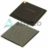
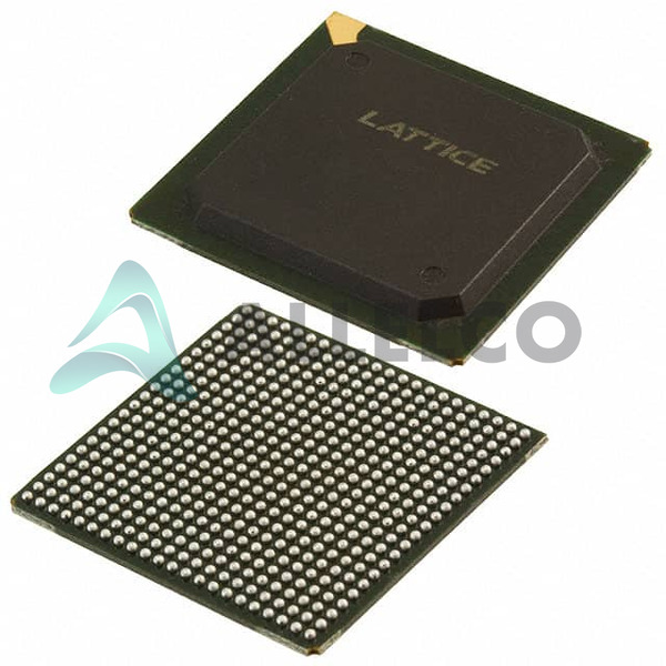
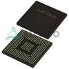
LCMXO2-7000HC-5FG484I (1)

Manufacturer Part Number

LCMXO2-7000HC-5FG484I

Manufacturer

Lattice Semiconductor

Introduction

The LCMXO2-7000HC-5FG484I is a high-performance FPGA from Lattice Semiconductor's MachXO2 series designed for embedded systems integration.

Product Features and Performance

Field Programmable Gate Array

6864 Logic Elements/Cells

858 LABs/CLBs

245760 Total RAM Bits

334 Number of I/O

Surface Mount Mounting Type

Operating in the temperature range of -40°C ~ 100°C

Product Advantages

Optimized for low power consumption

High input and output pin count supporting complex designs

Robust thermal management suitable for variable operating environments

Key Technical Parameters

Voltage Supply: 2.375V ~ 3.465V

Package: 484-BBGA

Supply Device Package: 484-FBGA (23x23)

Quality and Safety Features

Operates effectively across a broad temperature range ensuring reliability

Compatibility

Compatible with a wide range of supply voltages and surface mount technology

Application Areas

Ideal for industrial, automotive, consumer electronics, and communications infrastructure

Product Lifecycle

Currently Active with a stable supply available. Long term availability without nearing discontinuation.

Several Key Reasons to Choose This Product

High logic capacity and extensive memory for complex design deployments

Flexible I/O count facilitating diverse application use cases

Sustainable operating features within harsh environments

End-to-end quality assurance from development to deployment

Frequently Asked Questions(FAQ)

How does the LCMXO2-7000HC-5FG484I compare to other MachXO2 devices in terms of logic capacity and I/O availability for mid-range FPGA applications?
The LCMXO2-7000HC-5FG484I delivers 6,864 logic elements and 334 general-purpose I/Os, positioning it above the base LCMXO2-1200 (1,280 LE) and below the LCMXO2-2500 (2,560 LE) within the same family. This makes it suitable for designs requiring moderate logic density and extensive peripheral interfacing, such as industrial control systems or sensor aggregation nodes. Its 334 I/O count is among the highest in the MachXO2 line, enabling direct connection to multiple parallel interfaces without requiring external multiplexers.
What are the key thermal and power implications of selecting the LCMXO2-7000HC-5FG484I in a -40°C to 100°C operating environment?
Operating across this wide temperature range places the LCMXO2-7000HC-5FG484I in automotive or industrial-grade applications where thermal cycling and ambient extremes are common. The device’s 100°C maximum junction temperature requires careful PCB layout with adequate copper pour and thermal vias under the FBGA package. Power consumption scales with switching activity and I/O load; at full utilization, dynamic power can exceed 50 mW, necessitating attention to clock gating and idle-state management to meet system-level thermal budgets.
In what scenarios would the LCMXO2-7000HC-5FG484I be preferred over an entry-level CPLD despite its higher cost and complexity?
The LCMXO2-7000HC-5FG484I offers significantly greater flexibility than a CPLD due to its larger RAM resources (245,760 bits), more complex routing architecture, and support for soft processors like LX4 or LX9 cores. It becomes advantageous when implementing state machines with deep memory, time-sensitive protocol handling such as PCIe or Ethernet MACs, or multi-channel data acquisition requiring FIFO buffering. Unlike CPLDs, it supports partial reconfiguration and advanced timing models, which are critical in adaptive systems or test-and-measurement equipment.
How should designers evaluate whether the LCMXO2-7000HC-5FG484I’s voltage supply range (2.375V to 3.465V) aligns with their target system’s power architecture?
The LCMXO2-7000HC-5FG484I operates over a broad supply window typical of 3.3V systems but includes compatibility with lower-voltage domains down to 2.375V. Designers must ensure that all I/O banks sharing a common voltage rail fall within this range and that level-shifting circuitry is used appropriately when interfacing with sub-2.375V logic such as 1.8V microcontrollers. Additionally, brown-out protection and power sequencing must account for the upper limit near 3.465V, especially if derived from unregulated sources like batteries or solar inputs.
What impact does the LCMXO2-7000HC-5FG484I’s 484-FBGA packaging have on board design and manufacturability?
The 23×23 mm 484-ball FBGA package demands precise PCB fabrication tolerances—typically Class 2 or better—with via-in-pad or microvias for fine-pitch escape routing. Solder paste stenciling and reflow profiling are critical due to the high pin count and tight pitch (0.8 mm). Thermal performance benefits from a solid ground plane beneath the array, but warpage risk increases with thick boards or asymmetric layer stacks. Designers should verify assembly house capabilities before committing to this footprint.
Can the LCMXO2-7000HC-5FG484I support real-time clocking and synchronization requirements common in distributed industrial networks?
Yes, the LCMXO2-7000HC-5FG484I includes dedicated Phase-Locked Loop (PLL) resources that enable frequency synthesis and jitter reduction essential for synchronous protocols like EtherCAT or PROFINET IRT. With up to four PLLs per device and programmable output dividers, it can generate multiple phase-aligned clocks from a single reference. However, achieving sub-microsecond synchronization demands careful placement of clock nets, minimized trace lengths, and adherence to skew budgets during implementation.
How does the number of LABs (Logic Array Blocks) in the LCMXO2-7000HC-5FG484I influence place-and-route efficiency compared to smaller MachXO2 variants?
The LCMXO2-7000HC-5FG484I contains 858 LABs organized into 168 CLBs, providing ample granularity for modular design partitioning. This structure reduces congestion during place-and-route compared to denser devices, as signals tend to localize within functional blocks. However, large combinatorial paths spanning multiple LABs may introduce longer delays; thus, timing closure relies on proper constraint definition and incremental compilation strategies rather than relying solely on device headroom.
What considerations apply when integrating the LCMXO2-7000HC-5FG484I with external SRAM or flash memory for configuration storage?
The LCMXO2-7000HC-5FG484I supports serial configuration via SPI using external flash, which reduces pin usage but introduces boot-up latency. When using SPI flash, ensure signal integrity on MOSI/MISO/SCK lines—especially in noisy environments—and validate hold times relative to the device’s setup requirements (typically <10 ns). For dual-bank configurations supporting in-system updates, additional GPIO pins are needed for bank selection and status monitoring, increasing I/O overhead.
Why might a designer choose the LCMXO2-7000HC-5FG484I over an ASIC prototype despite longer development cycles?
The LCMXO2-7000HC-5FG484I enables rapid iteration without mask costs, ideal for validating algorithms, testing interface protocols, or prototyping user-defined logic before committing to custom silicon. Its reprogrammability allows hardware fixes post-deployment, extending product lifecycle. Given its moderate gate count and embedded flash, it strikes a balance between flexibility and power efficiency—superior to discrete logic solutions while avoiding ASIC NRE and volume pricing disadvantages.
How does the Moisture Sensitivity Level (MSL) rating of 3 for the LCMXO2-7000HC-5FG484I affect storage and lead time planning?
MSL 3 indicates the LCMXO2-7000HC-5FG484I must be stored in dry conditions and soldered within 168 hours after humidification unless properly baked. This impacts supply chain logistics, particularly for long-lead builds or field replacements. Inventory management should include humidity-controlled environments or desiccant packaging, and procurement schedules must account for potential requalification steps if shelf life exceeds recommended limits.
What role do the embedded 245,760-bit RAM blocks play in implementing packet buffering or data logging with the LCMXO2-7000HC-5FG484I?
These configurable block RAMs allow creation of FIFOs, dual-port memories, or lookup tables directly within the FPGA fabric. For example, a 32-bit wide 64-entry FIFO consumes ~1 KB of RAM and can buffer 16 full packets of 32 bytes each, mitigating bursty traffic between asynchronous domains. The LCMXO2-7000HC-5FG484I’s distributed RAM architecture avoids external memory dependencies, reducing BOM cost and improving reliability in harsh environments.
Is the LCMXO2-7000HC-5FG484I suitable for battery-powered edge devices where quiescent current must remain below 1 mA?
While the LCMXO2-7000HC-5FG484I consumes minimal static power (<1 µA in standby), active mode draw depends heavily on configuration, I/O loads, and clock frequencies. Achieving sub-milliamp average current requires aggressive sleep modes, disabling unused PLLs, minimizing toggle rates, and using low-swing I/O standards. In such cases, alternative ultra-low-power FPGAs or ASSPs may offer better efficiency, but the LCMXO2-7000HC-5FG484I remains viable with disciplined power-aware design.
How does the LCMXO2-7000HC-5FG484I handle ESD protection during assembly and field operation?
The device integrates standard human-body model (HBM) ESD protection diodes at each I/O pin, rated typically at ±2 kV. However, this is not equivalent to isolated ESD circuits found in some industrial modules. During board handling, conformal coating or TVS diodes on critical lines may be necessary. In end applications exposed to electrostatic events (e.g., handheld tools), external protection components are strongly advised.
What verification steps are recommended before deploying firmware on the LCMXO2-7000HC-5FG484I in safety-critical systems?
Functional simulation alone is insufficient; formal timing analysis, power estimation, and fault injection testing should complement RTL validation. Use static timing analysis (STA) to confirm worst-case delays meet deadlines, and perform corner-based simulations (-40°C, 100°C, min/max VCC) to validate robustness. Additionally, verify configuration bitstream integrity through CRC checks and implement watchdog timers to recover from runtime errors.
Can the LCMXO2-7000HC-5FG484I coexist with other Lattice devices in a multi-chip system without bus contention?
Yes, provided I/O standards and voltage levels are compatible across devices. The LCMXO2-7000HC-5FG484I supports LVCMOS and LVTTL up to 3.3V, so it can interface with newer Lattice FPGAs using similar I/O banks. Bidirectional buffers or tristate control logic must be managed carefully to prevent shoot-through currents, especially when sharing buses during power-up sequences. Decoupling and impedance matching become more critical in multi-device topologies.
How does the absence of a built-in ADC impact signal conditioning tasks typically handled by mixed-signal FPGAs?
The LCMXO2-7000HC-5FG484I lacks integrated ADCs, requiring external front-end circuits for analog-to-digital conversion. This shifts responsibility to external ICs but allows customization of sampling rates, resolution, and anti-aliasing filters. Designers gain flexibility in choosing ADC types (SAR, Sigma-Delta) based on application needs, though they must allocate FPGA resources to digital filtering and decimation instead of relying on on-die processing.
What documentation and development tools are essential for efficiently programming the LCMXO2-7000HC-5FG484I?
Lattice Diamond or Radiant IDE is required for synthesis, place-and-route, and bitstream generation. The software supports Verilog/VHDL and includes timing analysis tools. Hardware debugging benefits from Lattice Programming Pod or third-party JTAG adapters capable of handling high-density BGA packages. Reference designs and IP cores (e.g., UART, I2C, SPI controllers) accelerate integration, especially when targeting legacy interfaces in modern systems.
How does the LCMXO2-7000HC-5FG484I’s RoHS3 compliance influence material selection and regulatory reporting?
RoHS3 compliance ensures the LCMXO2-7000HC-5FG484I meets updated restrictions on substances like phthalates and mercury, aligning with EU directives. Manufacturers must provide SCIP notifications for SVHCs and maintain documentation for conflict minerals sourcing. This simplifies global market access but requires traceability throughout the supply chain, particularly when combining with non-compliant passive components or connectors in final assemblies.

Parts with Similar Specifications

The three parts on the right have similar specifications to Lattice Semiconductor Corporation LCMXO2-7000HC-5FG484I

Product Attribute LCMXO2-7000HC-5FG484C LCMXO2-7000HC-5TG144I LCMXO2-7000HC-4TG144I LCMXO2-7000HC-5TG144C
Part Number LCMXO2-7000HC-5FG484C LCMXO2-7000HC-5TG144I LCMXO2-7000HC-4TG144I LCMXO2-7000HC-5TG144C
Manufacturer Lattice Semiconductor Corporation Lattice Semiconductor Corporation Lattice Semiconductor Corporation Lattice Semiconductor Corporation
Total RAM Bits - - - -
Number of LABs/CLBs - - - -
Supplier Device Package - 196-NFBGA (12x12) 16-PDIP 64-VQFN (9x9)
Series - - - -
Base Product Number - DAC34H84 MAX500 ADS62P42
Number of I/O - - - -
Mounting Type - Surface Mount Through Hole Surface Mount
Package / Case - 196-LFBGA 16-DIP (0.300', 7.62mm) 64-VFQFN Exposed Pad
Package - Tape & Reel (TR) Tube Tape & Reel (TR)
Operating Temperature - -40°C ~ 85°C 0°C ~ 70°C -40°C ~ 85°C
Voltage - Supply - - - -
Number of Logic Elements/Cells - - - -

LCMXO2-7000HC-5FG484I Datasheet PDF

Download LCMXO2-7000HC-5FG484I pdf datasheets and Lattice Semiconductor Corporation documentation for LCMXO2-7000HC-5FG484I - Lattice Semiconductor Corporation.

Datasheets
MachXO2 Family Datasheet.pdf
PCN Packaging
All Dev Pkg Mark Chg 12/Nov/2018.pdf
PCN Assembly/Origin
Alternate Assembly/Test Site 14/Apr/2014.pdf
PCN Design/Specification
Datasheet Chg 21/Mar/2016.pdf Multiple Devices Cu Wire 01/Jul/2013.pdf
PCN Other
I2C Read-Back Failure Feb/2015.pdf
Getting Started Guide
Product Selector Guide.pdf

Customer Reviews

Evaluation: 10 Articles

  • Nath***rooks
    Jun 11, 2026

    Installed this power component in a converter board. Output remained stable under different load conditions and thermal performance was better than expected.

  • Dani***alkerTech
    Jun 1, 2026

    Product works, but setup took more effort than expected. Once configured the MCU ran reliably, although documentation support felt older compared with newer platforms. Fine for maintenance projects.

  • Yuki***aka88
    May 26, 2026

    信号通信プロジェクトでこのRS-485トランシーバーを使用しました。設置は簡単で、長距離ケーブルでも通信は安定していました。消費電力も、以前使用していたものより低くなっています。

  • Stev***aker
    May 20, 2026

    Solid diode for power rectification. Works well in switching circuits.

  • Bran***Lewis
    May 11, 2026

    Compact FPGA with good performance. Suitable for basic signal processing tasks.

  • Oliv***arris
    May 7, 2026

    Reliable I/O expander. Works well in embedded control applications.

  • Jess***Jones
    Apr 17, 2026

    It offers good value for the price, and the specifications match the description. I’ve been using it for two days with no issues, and I’ll definitely buy it again if I need it in the future.

  • Mich***Smith
    Apr 17, 2026

    Shipping was on time, the component pins are neatly aligned, and I tested 10 of them with a multimeter—all readings were within the specified range. Highly recommended.

  • Aman***arris
    Apr 3, 2026

    It was great—the entire process, from placing the order to receiving the package, went very smoothly. The components were consistent, the price was fair, and I had a very pleasant shopping experience.

  • Mike***nch
    Apr 3, 2026

    Better than expected! The resistance and capacitance readings were spot-on, and it passed the test on the first try. The service was reliable, and the packaging was thoughtful—I highly recommend it.

Write a Review

Your Email address will not be published.

Shipment

Delivery Time

In-stock items can be shipped within 24 hours. Some parts will be arranged for delivery within 1-2 days from the date all items arrive at our warehouse. And Allelco ships order once a day at about 17:00, except Sunday. Once the goods are shipped, the estimated delivery time depends on the shipping methods and Delivery destination. The table below shows are the logistic time for some common countries.

Delivery Cost

  1. Use your express account for shipment if you have one.
  2. Use our account for the shipment. Refer to the table below for the approximate charges.
(Different time frame / countries / package size has different price.)

Delivery Method

  1. Global Common Shipment by DHL / UPS / FedEx / TNT / EMS / SF we support.
  2. Others more shipping ways, please get in touch with your customer manager.

Common Countries Logistic Time Reference
Region Country Logistic Time(Day)
America United States 5
Brazil 7
Europe Germany 5
United Kingdom 4
Italy 5
Oceania Australia 6
New Zealand 5
Asia India 4
Japan 4
Middle East Israel 6
DHL & FedEx Shipment Charges Reference
Shipment charges(KG) Reference DHL(USD$)
0.00kg-1.00kg USD$30.00 - USD$60.00
1.00kg-2.00kg USD$40.00 - USD$80.00
2.00kg-3.00kg USD$50.00 - USD$100.00
Note:
The above table is for reference only. There may have some data bias for the uncontrollable factors.
Contact us if you have any questions.
  • QC (Quality Warranty)
  • Payment Support
  • Packaging
  • Certifications & Memberships

QC (Quality Warranty)

Allelco is committed to exceeding customer expectations through customer service excellence, order accuracy, and on-time delivery.
This is achieved through our commitment to the continual improvement of our processes, services, and products.


Strict quality inspection builds a solid foundation for electronic component quality.
  1. Visual inspection
  2. Performance testing and reliability verification
  3. Standardized full-process testing
  4. Precise control of every parameter
We eliminate defective components and ensure the stable operation of electronic devices through professional quality standards.

Payment Support

The payment method can be chosen from the methods shown below: Wire Transfer (T/T, Bank Transfer), Western Union, Credit card, PayPal.
  • HKBea
  • Paypal
  • MasterCard
  • Western-Union
  • VISA
Stable Delivery, Sincere Partnership — Your Faithful Supply Chain Partner
  • Efficient Supply Management
  • Cost-Saving Procurement
  • Fast Sourcing & Delivery
Contact us if you have any questions.

Packaging

Electrostatic Discharge Protection and Handling

All electrostatic-sensitive components are handled in accordance with electrostatic discharge control procedures. The products are hermetically sealed in anti-static safe packaging to prevent electrostatic damage. Appropriate labeling is also applied for identification and traceability. This ensures product integrity during storage, handling and transportation.


ESD

Certifications & Memberships

Third-party certified, strict quality control. Our certification
  • ISO 9001: 2015
  • ISO 13485: 2016
  • ISO 14001: 2015
  • ISO 28000: 2007
  • ISO 45001: 2018
  • GB/T 27922-2011
  • SMTA
  • IPC
  • ESD
  • PSMA
LCMXO2-7000HC-5FG484I Image

LCMXO2-7000HC-5FG484I

Lattice Semiconductor Corporation
32D-LCMXO2-7000HC-5FG484I

Want a better price? Add to Cart and Submit RFQ now, we'll contact you immediately.

0 RFQ
Shopping cart (0 Items)
It is empty.
Compare List (0 Items)
It is empty.
Feedback

Your feedback matters! At Allelco, we value the user experience and strive to improve it constantly.
Please share your comments with us via our feedback form, and we'll respond promptly.
Thank you for choosing Allelco.

Subject
E-mail
Comments
Captcha
Drag or click to upload file
Upload File
types: .xls, .xlsx, .doc, .docx, .jpg, .png and .pdf.
Max file size: 10MB