
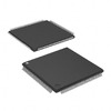
Manufacturer Part Number
LCMXO2-7000HC-4FTG256C
Manufacturer
Lattice Semiconductor
Introduction
The LCMXO2-7000HC-4FTG256C is a high-capacity, low-power FPGA from Lattice Semiconductor's MachXO2 series. It offers a versatile and reconfigurable platform for a wide range of embedded applications, enabling designers to quickly implement custom logic and accelerate system performance.
Product Features and Performance
858 Logic Blocks (LABs)
6,864 Logic Cells
245,760 Total RAM Bits
206 I/O Pins
Operating voltage range: 2.375V to 3.465V
Operating temperature range: 0°C to 85°C
Product Advantages
Flexible and programmable logic for customized solutions
Low power consumption for energy-efficient designs
Robust performance and reliability for critical applications
Fast time-to-market with easy-to-use development tools
Key Reasons to Choose This Product
Scalable and feature-rich FPGA solution
Proven reliability and long-term availability
Excellent value proposition for cost-sensitive projects
Comprehensive ecosystem of development tools and IP cores
Quality and Safety Features
Industrial-grade quality and reliability
Compliance with various safety and regulatory standards
Compatibility
The LCMXO2-7000HC-4FTG256C is compatible with a wide range of embedded systems, peripheral interfaces, and development platforms.
Application Areas
Industrial automation and control
Automotive electronics
Medical equipment
Wireless and IoT applications
Consumer electronics
Product Lifecycle
The LCMXO2-7000HC-4FTG256C is an active product in our website's sales team's portfolio. There are several equivalent and alternative models available in the MachXO2 series, such as the LCMXO2-7000HE-4FTG256C and LCMXO2-7000HC-5TG256C. Customers are advised to contact our website's sales team for the latest product information and availability.
 LCMXO2-7000HC-4TG144CLattice Semiconductor CorporationIC FPGA 114 I/O 144TQFP
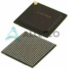 LCMXO2-7000HC-4FG484CLattice Semiconductor CorporationIC FPGA 334 I/O 484FBGA
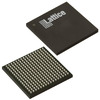 LCMXO2-7000HC-5BG256ILattice Semiconductor CorporationIC FPGA 206 I/O 256CABGA
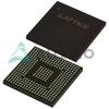 LCMXO2-7000HC-4BG332CLattice Semiconductor CorporationIC FPGA 278 I/O 332CABGA
 LCMXO2-7000HC-4FTG256ILattice Semiconductor CorporationIC FPGA 206 I/O 256FTBGA
 LCMXO2-7000HCLattice


