
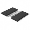
 SN65LVDT122DG4Texas InstrumentsIC CROSSPOINT SW 1 X 2:2 16SOIC
 SN65LVDT14PWRTexas InstrumentsIC TRANSCEIVER HALF 1/4 20TSSOP
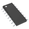
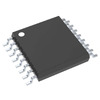 SN65LVDT122PWRG4Texas InstrumentsIC CROSSPOINT SW 1 X 2:2 16TSSOP
 SN65LVDT14QPWREPTexas Instruments
- Dani***alkerTech
- Jun 1, 2026
HomeProductsIntegrated Circuits (ICs)Logic - Signal Switches, Multiplexers, DecodersSN65LVDT125ADBTR

Image may be representation.
See specifications for product details.
See specifications for product details.
- EXPRESS OPTION
- Payment method
SN65LVDT125ADBTR - Texas Instruments
- Manufacturer Part Number
- SN65LVDT125ADBTR
- Manufacturer
- Texas Instruments
- Allelco Part Number
- 98D-SN65LVDT125ADBTR
- Warranty
- 1 Year Allelco Warranty - Find out more
- Stock Status:
- 13,278 pcs available, New & Original
- Parts Description
- IC CROSSPOINT SW 1 X 4:4 38TSSOP
- Package
- 38-TSSOP
- Data sheet
-
SN65LVDT125ADBT.pdf
HTML Datasheet
SN65LVDS125A, SN65LVDT125A.pdf
- RoHs Status
- ROHS3 Compliant
- Our certification
- In stock: 13278


