View All

Please refer to the English Version as our Official Version.Return

Europe
France(Français) Germany(Deutsch) Italy(Italia) Russian(русский) Poland(polski) Czech(Čeština) Luxembourg(Lëtzebuergesch) Netherlands(Nederland) Iceland(íslenska) Hungarian(Magyarország) Spain(español) Portugal(Português) Turkey(Türk dili) Bulgaria(Български език) Ukraine(Україна) Greece(Ελλάδα) Israel(עִבְרִית) Sweden(Svenska) Finland(Svenska) Finland(Suomi) Romania(românesc) Moldova(românesc) Slovakia(Slovenská) Denmark(Dansk) Slovenia(Slovenija) Slovenia(Hrvatska) Croatia(Hrvatska) Serbia(Hrvatska) Montenegro(Hrvatska) Bosnia and Herzegovina(Hrvatska) Lithuania(lietuvių) Spain(Português) Switzerland(Deutsch) United Kingdom(English)
Asia/Pacific
Japan(日本語) Korea(한국의) Thailand(ภาษาไทย) Malaysia(Melayu) Singapore(Melayu) Vietnam(Tiếng Việt) Philippines(Pilipino)
Africa, India and Middle East
United Arab Emirates(العربية) Iran(فارسی) Tajikistan(فارسی) India(हिंदी) Madagascar(malaɡasʲ)
South America / Oceania
New Zealand(Maori) Brazil(Português) Angola(Português) Mozambique(Português)
North America
United States(English) Canada(English) Haiti(Ayiti) Mexico(español)
HomeProductsIntegrated Circuits (ICs)Logic - Signal Switches, Multiplexers, DecodersSN65LVDT125DBT
SN65LVDT125DBT Image
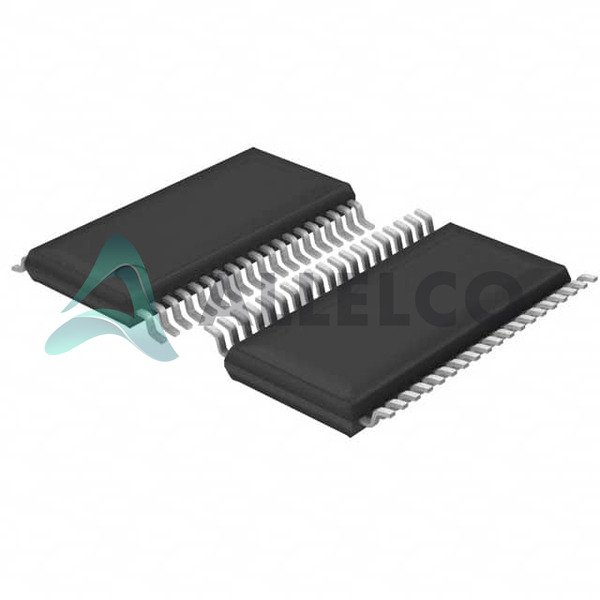
Image may be representation.
See specifications for product details.
EXPRESS OPTION
Payment method

SN65LVDT125DBT - Texas Instruments

Manufacturer Part Number
SN65LVDT125DBT
Manufacturer
Texas Instruments
Allelco Part Number
98D-SN65LVDT125DBT
Warranty
1 Year Allelco Warranty - Find out more
Stock Status:
44,321 pcs available, New & Original
Parts Description
IC SWTCH CRSSPT LVDS 4X4 38TSSOP
Package
38-TSSOP
Data sheet
-
RoHs Status
 
Our certification
In stock: 44321
  • Unit Price: $4.17
  • Subtotal: $0.00

Want a better price?
Add to Cart and Submit RFQ now, we'll contact you immediately.

Quantity Unit Price Ext. Price
1+ $4.17 $4.17
The above prices does not include taxes and freight rates, which will be calculated on the order pages.

Specifications

SN65LVDT125DBT Tech Specifications
Texas Instruments - SN65LVDT125DBT technical specifications, attributes, parameters and parts with similar specifications to Texas Instruments - SN65LVDT125DBT

Product Attribute Attribute Value
Manufacturer Texas Instruments
Voltage Supply Source Single Supply
Voltage - Supply 3V ~ 3.6V
Type Crosspoint Switch
Supplier Device Package 38-TSSOP
Series 65LVDT
Package / Case 38-TFSOP (0.173", 4.40mm Width)
Product Attribute Attribute Value
Package Tube
Operating Temperature -40°C ~ 85°C
Mounting Type Surface Mount
Independent Circuits 1
Current - Output High, Low -
Circuit 1 x 4:4
Base Product Number 65LVDT125

Environmental & Export Classifications

ATTRIBUTE DESCRIPTION
RoHs Status RoHS non-compliant
Moisture Sensitivity Level (MSL) 1 (Unlimited)
REACH Status REACH Unaffected
ECCN 5A991B1
HTSUS 8542.39.0001

Frequently Asked Questions(FAQ)

How does the SN65LVDT125DBT handle signal integrity when routing multiple LVDS channels through a single crosspoint switch in a 3.3V system?
The SN65LVDT125DBT maintains differential signaling integrity across all four input-to-output paths using its integrated LVDS transceivers, which feature built-in termination and controlled skew characteristics of less than 0.2 ns typical. This ensures minimal degradation of signal rise times and eye diagram quality, even when switching between multiple high-speed serial links at data rates up to 1.25 Gbps. In a 3.3V supply environment, the device operates within its specified voltage range of 3V to 3.6V, maintaining consistent output levels and receiver thresholds to prevent misalignment in noisy environments.
What design considerations are critical when cascading the SN65LVDT125DBT with other logic devices that have different input voltage thresholds?
When interfacing the SN65LVDT125DBT with downstream CMOS or TTL logic, level translation must be carefully evaluated due to its LVDS output swing (typically 350 mV differential). Since LVDS outputs do not directly drive standard CMOS inputs, additional circuitry such as resistive dividers or dedicated level translators may be required unless the receiving device has compatible low-threshold inputs. The 3.3V single-supply operation simplifies power management but demands attention to input compatibility to avoid undefined states during switching transitions.
Can the SN65LVDT125DBT support hot-swapping or dynamic reconfiguration of input sources without causing bus contention?
The SN65LVDT125DBT includes internal protection diodes on each input line, providing ESD immunity up to ±15 kV per IEC 61000-4-2, but it does not inherently support true hot-plug capability. While brief glitches may occur during rapid source switching, the device’s control interface—driven by standard digital signals—allows deterministic switching via GPIOs without risking bus contention if outputs are tri-stated during transitions. Careful timing coordination between control logic and enable/disable sequences is recommended for robust system integration.
How does thermal performance impact the reliability of the SN65LVDT125DBT in compact PCB layouts?
Operating the SN65LVDT125DBT within its -40°C to +85°C junction temperature range ensures stable operation under most industrial conditions, but power dissipation must be monitored. With typical quiescent current around 3.5 mA per channel and dynamic losses proportional to switching frequency, total package dissipation can reach ~125 mW in dense designs. The 38-pin TSSOP package offers limited thermal relief compared to larger footprints; therefore, adequate copper pour and airflow should be implemented to prevent localized heating, especially when all four channels operate simultaneously at full bandwidth.
What are the limitations of using the SN65LVDT125DBT in applications requiring galvanic isolation?
The SN65LVDT125DBT lacks any form of electrical isolation between input and output stages, making it unsuitable for systems where safety or noise immunity requires barrier separation. Its operation relies on shared ground references, so floating domains or isolated power supplies cannot be bridged directly without external isolators such as optical couplers or digital isolators. Applications involving medical equipment, automotive safety systems, or industrial automation with hazardous voltages must incorporate additional isolation components before or after this crosspoint switch.
How does the propagation delay of the SN65LVDT125DBT affect synchronization in multi-lane data transmission systems?
The SN65LVDT125DBT exhibits uniform propagation delays across channels—typically 0.8 ns maximum—which helps maintain alignment between parallel data lanes. However, cumulative skew over long traces or across multiple stages can introduce timing mismatches exceeding acceptable jitter budgets in high-speed protocols like PCIe or Ethernet. Designers should account for this delay when calibrating deskew algorithms or allocating equalization margins, particularly in systems where lane-to-lane phase matching is critical for error-free decoding at speeds approaching 1.25 Gbps.
What testing methodology ensures reliable functionality of the SN65LVDT125DBT under real-world EMI conditions?
To validate robustness against electromagnetic interference, the SN65LVDT125DBT should undergo conducted and radiated emission testing according to IEC 61000-4-3 and -4-6 standards. Additionally, functional stress tests simulating simultaneous switching of multiple outputs while injecting common-mode noise into the differential lines help verify receiver margin compliance. Given its use in point-to-point serial links, eye mask analysis at the far end of simulated PCB trace lengths provides empirical validation of signal integrity, confirming that bit error rates remain below 1E-12 under worst-case environmental conditions.
How does the Moisture Sensitivity Level (MSL) rating of the SN65LVDT125DBT influence storage and handling procedures?
Classified as MSL 1, the SN65LVDT125DBT is exempt from moisture-sensitive handling requirements, meaning it can be stored indefinitely at room temperature without baking prior to reflow soldering. This simplifies inventory management and reduces lead times for prototyping or production builds, especially in environments with fluctuating humidity. However, standard ESD precautions must still be followed due to its sensitive CMOS inputs, despite the absence of special packaging beyond standard tube delivery.
What trade-offs exist between bandwidth utilization and power consumption when configuring the SN65LVDT125DBT for partial-channel operation?
Reducing active channels from four to one decreases dynamic power proportionally, lowering total supply current from ~14 mA to approximately 3.5 mA at 1.25 Gbps, while maintaining full LVDS signaling fidelity. However, unused inputs must be terminated properly to avoid reflections, and output drivers should be disabled if not needed to minimize crosstalk. This balance allows optimized energy usage in battery-powered or thermally constrained systems without sacrificing signal quality, provided layout parasitics are minimized through proper impedance control.
How does the absence of I2C or SPI control interfaces limit configuration flexibility in the SN65LVDT125DBT compared to software-configurable alternatives?
Unlike programmable crosspoint switches such as those using FPGA-based routing or digital ICs with serial interfaces, the SN65LVDT125DBT employs hardwired internal routing controlled exclusively via external enable pins. This eliminates firmware complexity but restricts real-time reconfiguration; once set, the topology remains fixed until hardware changes. For applications requiring dynamic path selection based on system state, an alternative solution may be preferable, though the SN65LVDT125DBT excels in fixed-multiplexing scenarios where simplicity and deterministic behavior outweigh configurability needs.
What role does package parasitics play in signal integrity when using the 38-TSSOP version of the SN65LVDT125DBT?
The 38-pin TSSOP package introduces parasitic inductance and capacitance inherent to fine-pitch surface-mount geometries, which can distort high-frequency LVDS edges above 500 MHz. These effects become significant when traces are routed perpendicularly across the package width or when vias disrupt return paths. To mitigate this, designers should minimize loop areas for return currents, use adjacent ground planes, and avoid placing bypass capacitors too far from the device pads—ideally within 2 mm—to ensure stable power delivery and preserve signal integrity up to the rated bandwidth.
Why might a designer choose the SN65LVDT125DBT over discrete multiplexer solutions for LVDS routing?
Compared to building a custom mux from discrete analog switches and buffers, the SN65LVDT125DBT integrates matched transceivers, reduced skew, and built-in ESD protection in a single component, reducing board space, bill-of-materials count, and calibration effort. It also supports native LVDS-to-LVDS routing without level shifting, preserving signal strength and timing margins. For four-input, four-output configurations operating at 1 Gbps+, this integration delivers superior reliability and easier compliance with EMI/EMC regulations due to controlled impedance and shielding benefits of a monolithic design.
How does RoHS non-compliance status of the SN65LVDT125DBT affect global market deployment?
As a RoHS non-compliant part, the SN65LVDT125DBT cannot be sold into markets enforcing strict hazardous substance restrictions, such as the European Union under Directive 2011/65/EU, unless exemptions apply. This limits its availability through mainstream distributors and complicates supply chain logistics for projects targeting CE marking or similar certifications. Engineers considering this device must verify local regulatory requirements early in development and anticipate potential need to source compliant alternatives like newer TI parts such as the SN65HVDT125, which meets current environmental standards.
What diagnostic features does the SN65LVDT125DBT provide for troubleshooting failed links in production environments?
The SN65LVDT125DBT offers no internal diagnostic registers or loopback modes, limiting self-test capabilities. External test points or protocol analyzers are typically required to isolate faults such as stuck-at states or incorrect routing. However, its low propagation delay and consistent output swing allow faster fault detection using time-domain reflectometry or eye pattern measurements. System-level diagnostics—such as monitoring receiver lock indicators from downstream PHYs—are essential for effective root-cause analysis in deployed systems using this crosspoint switch.
How does the ECCN classification (5A991B1) influence export controls for the SN65LVDT125DBT?
Classified under ECCN 5A991B1, the SN65LVDT125DBT falls under U.S. Commerce Control List Category 5, Part 2, related to information security items. This designation implies potential export restrictions to certain countries or end-users without proper licenses, particularly when incorporated into defense or telecommunications equipment. Importers and integrators should consult BIS guidelines and conduct end-use checks to avoid compliance violations, especially in international supply chains where dual-use concerns may trigger additional screening.
What impact does uncontrolled trace length mismatch have on the SN65LVDT125DBT performance in multi-drop configurations?
Although the SN65LVDT125DBT is designed for point-to-point connections rather than multi-drop buses, asymmetrical routing between inputs and outputs introduces differential skew exceeding the device’s 0.2 ns specification. At 1.25 Gbps, even 50 ps of mismatch causes significant intersymbol interference, degrading eye height and increasing bit error rates. Therefore, traces must be length-matched within ±50 mil to preserve timing margins, and stubs or vias should be avoided to prevent impedance discontinuities that compound signal degradation.
How should decoupling capacitors be sized and placed to stabilize the SN65LVDT125DBT under transient load conditions?
A 100 nF ceramic capacitor should be placed within 1 mm of the VCC and GND pins of the SN65LVDT125DBT, supplemented by a 1 µF bulk capacitor near the power entry point. This combination suppresses high-frequency noise from switching outputs and stabilizes the 3.3V rail against inductive kickback during simultaneous channel activation. Low-ESR MLCCs with X7R dielectric are preferred for stability across the operating temperature range, ensuring consistent reference levels for both transmitters and receivers despite dynamic current surges.

Parts with Similar Specifications

The three parts on the right have similar specifications to Texas Instruments SN65LVDT125DBT

Product Attribute SN65LVDT125ADBT SN65LVDT125ADBTRG4 SN65LVDT125ADBTR SN65LVDT125ADBTG4
Part Number SN65LVDT125ADBT SN65LVDT125ADBTRG4 SN65LVDT125ADBTR SN65LVDT125ADBTG4
Manufacturer Texas Instruments Texas Instruments Texas Instruments Texas Instruments
Voltage - Supply - - - -
Type - - - -
Circuit - - - -
Package - Tape & Reel (TR) Tube Tape & Reel (TR)
Series - - - -
Base Product Number - DAC34H84 MAX500 ADS62P42
Current - Output High, Low - - - -
Supplier Device Package - 196-NFBGA (12x12) 16-PDIP 64-VQFN (9x9)
Operating Temperature - -40°C ~ 85°C 0°C ~ 70°C -40°C ~ 85°C
Voltage Supply Source - - - -
Package / Case - 196-LFBGA 16-DIP (0.300', 7.62mm) 64-VFQFN Exposed Pad
Independent Circuits - - - -
Mounting Type - Surface Mount Through Hole Surface Mount

Customer Reviews

Evaluation: 10 Articles

  • Dani***alkerTech
    Jun 1, 2026

    Product works, but setup took more effort than expected. Once configured the MCU ran reliably, although documentation support felt older compared with newer platforms. Fine for maintenance projects.

  • Yuki***aka88
    May 26, 2026

    信号通信プロジェクトでこのRS-485トランシーバーを使用しました。設置は簡単で、長距離ケーブルでも通信は安定していました。消費電力も、以前使用していたものより低くなっています。

  • Stev***aker
    May 20, 2026

    Solid diode for power rectification. Works well in switching circuits.

  • Bran***Lewis
    May 11, 2026

    Compact FPGA with good performance. Suitable for basic signal processing tasks.

  • Oliv***arris
    May 7, 2026

    Reliable I/O expander. Works well in embedded control applications.

  • Jess***Jones
    Apr 17, 2026

    It offers good value for the price, and the specifications match the description. I’ve been using it for two days with no issues, and I’ll definitely buy it again if I need it in the future.

  • Mich***Smith
    Apr 17, 2026

    Shipping was on time, the component pins are neatly aligned, and I tested 10 of them with a multimeter—all readings were within the specified range. Highly recommended.

  • Aman***arris
    Apr 3, 2026

    It was great—the entire process, from placing the order to receiving the package, went very smoothly. The components were consistent, the price was fair, and I had a very pleasant shopping experience.

  • Mike***nch
    Apr 3, 2026

    Better than expected! The resistance and capacitance readings were spot-on, and it passed the test on the first try. The service was reliable, and the packaging was thoughtful—I highly recommend it.

  • Daic***K.
    Mar 23, 2026

    Very good. No issue after long time testing.

Write a Review

Your Email address will not be published.

Shipment

Delivery Time

In-stock items can be shipped within 24 hours. Some parts will be arranged for delivery within 1-2 days from the date all items arrive at our warehouse. And Allelco ships order once a day at about 17:00, except Sunday. Once the goods are shipped, the estimated delivery time depends on the shipping methods and Delivery destination. The table below shows are the logistic time for some common countries.

Delivery Cost

  1. Use your express account for shipment if you have one.
  2. Use our account for the shipment. Refer to the table below for the approximate charges.
(Different time frame / countries / package size has different price.)

Delivery Method

  1. Global Common Shipment by DHL / UPS / FedEx / TNT / EMS / SF we support.
  2. Others more shipping ways, please get in touch with your customer manager.

Common Countries Logistic Time Reference
Region Country Logistic Time(Day)
America United States 5
Brazil 7
Europe Germany 5
United Kingdom 4
Italy 5
Oceania Australia 6
New Zealand 5
Asia India 4
Japan 4
Middle East Israel 6
DHL & FedEx Shipment Charges Reference
Shipment charges(KG) Reference DHL(USD$)
0.00kg-1.00kg USD$30.00 - USD$60.00
1.00kg-2.00kg USD$40.00 - USD$80.00
2.00kg-3.00kg USD$50.00 - USD$100.00
Note:
The above table is for reference only. There may have some data bias for the uncontrollable factors.
Contact us if you have any questions.
  • QC (Quality Warranty)
  • Payment Support
  • Packaging
  • Certifications & Memberships

QC (Quality Warranty)

Allelco is committed to exceeding customer expectations through customer service excellence, order accuracy, and on-time delivery.
This is achieved through our commitment to the continual improvement of our processes, services, and products.


Strict quality inspection builds a solid foundation for electronic component quality.
  1. Visual inspection
  2. Performance testing and reliability verification
  3. Standardized full-process testing
  4. Precise control of every parameter
We eliminate defective components and ensure the stable operation of electronic devices through professional quality standards.

Payment Support

The payment method can be chosen from the methods shown below: Wire Transfer (T/T, Bank Transfer), Western Union, Credit card, PayPal.
  • HKBea
  • Paypal
  • MasterCard
  • Western-Union
  • VISA
Stable Delivery, Sincere Partnership — Your Faithful Supply Chain Partner
  • Efficient Supply Management
  • Cost-Saving Procurement
  • Fast Sourcing & Delivery
Contact us if you have any questions.

Packaging

Electrostatic Discharge Protection and Handling

All electrostatic-sensitive components are handled in accordance with electrostatic discharge control procedures. The products are hermetically sealed in anti-static safe packaging to prevent electrostatic damage. Appropriate labeling is also applied for identification and traceability. This ensures product integrity during storage, handling and transportation.


ESD

Certifications & Memberships

Third-party certified, strict quality control. Our certification
  • ISO 9001: 2015
  • ISO 13485: 2016
  • ISO 14001: 2015
  • ISO 28000: 2007
  • ISO 45001: 2018
  • GB/T 27922-2011
  • SMTA
  • IPC
  • ESD
  • PSMA
SN65LVDT125DBT Image

SN65LVDT125DBT

Texas Instruments
98D-SN65LVDT125DBT

Want a better price? Add to Cart and Submit RFQ now, we'll contact you immediately.

0 RFQ
Shopping cart (0 Items)
It is empty.
Compare List (0 Items)
It is empty.
Feedback

Your feedback matters! At Allelco, we value the user experience and strive to improve it constantly.
Please share your comments with us via our feedback form, and we'll respond promptly.
Thank you for choosing Allelco.

Subject
E-mail
Comments
Captcha
Drag or click to upload file
Upload File
types: .xls, .xlsx, .doc, .docx, .jpg, .png and .pdf.
Max file size: 10MB