SN65LVDT14PWR (1)
Manufacturer Part Number
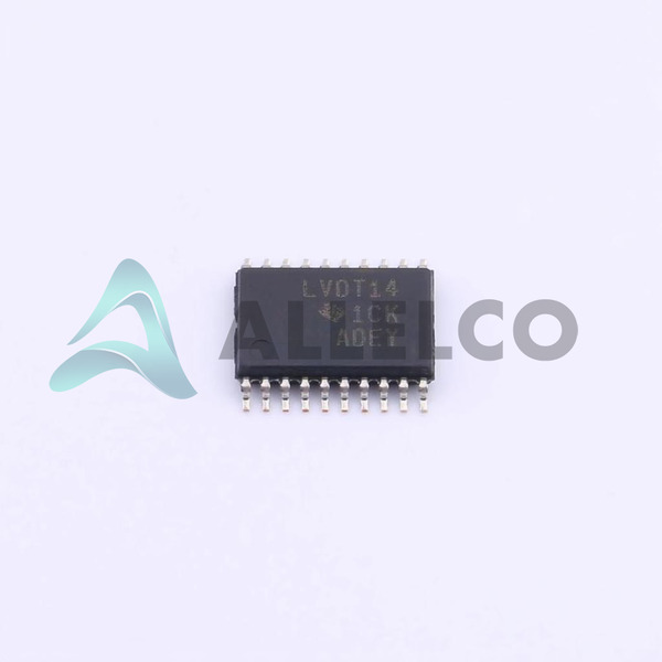
SN65LVDT14PWR
Manufacturer
Texas Instruments
Introduction
The SN65LVDT14PWR is a Low-Voltage Differential Signaling (LVDS) transceiver from Texas Instruments, designed for high-speed bidirectional point-to-point data transmission.
Product Features and Performance
LVDS Transceiver with 1 Driver and 4 Receivers
Half Duplex data communication
Operational Data Rate of 125Mbps
Low Voltage Operating Range of 3V to 3.6V
Supports wide Operating Temperature range from -40°C to 85°C
Surface Mount Technology for easy PCB integration
Offered in a 20-TSSOP Package for space-saving considerations
Product Advantages
High-speed data transfer capabilities
Robust against noise due to LVDS signaling
Low power consumption suitable for battery-operated devices
Suitable for high-temperature industrial applications
Key Technical Parameters
Data Rate: 125Mbps
Voltage Supply: 3V ~ 3.6V
Operating Temperature: -40°C ~ 85°C
Mounting Type: Surface Mount
Package / Case: 20-TSSOP
Quality and Safety Features
Manufactured by Texas Instruments, a leading semiconductor company
Compliance with industry safety and quality standards
Compatibility
Compatible with various LVDS standards
Interoperable with similar LVDS transceivers, receivers, and drivers
Application Areas
High-speed data communications
Telecommunications equipment
Networking devices and infrastructure
Computer peripherals
Industrial control and automation systems
Product Lifecycle
Currently in Active status
Not nearing discontinuation
Texas Instruments provides support for product longevity including availability of replacements or upgrades
Several Key Reasons to Choose This Product
Reliable data transfers at high speeds due to LVDS technology
Suitable for a wide range of operating temperatures, increasing applicability in harsh environments
Low power requirement enhances efficiency for energy-sensitive applications
Industry-standard package and mounting type allow for compatibility with existing systems
Backed by Texas Instruments' reputation for quality and longevity in the market


 SN65LVDT2DBVTTexas InstrumentsIC RECEIVER 0/1 SOT23-5
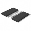 SN65LVDT125DBTTexas InstrumentsIC SWTCH CRSSPT LVDS 4X4 38TSSOP
 SN65LVDT14QPWREPTexas Instruments
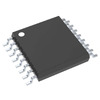 SN65LVDT122PWRG4Texas InstrumentsIC CROSSPOINT SW 1 X 2:2 16TSSOP


