


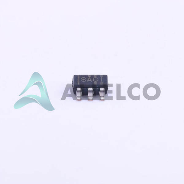
SN65LVDT2DBVR (1)
Manufacturer Part Number
SN65LVDT2DBVR
Manufacturer
Texas Instruments
Introduction
The SN65LVDT2DBVR is a high-speed differential receiver designed for applications requiring low-voltage differential signaling (LVDS) technology.
Product Features and Performance
Supports data rates up to 400Mbps
Applicable for point-to-point baseband data transmission
Low-voltage differential signaling for minimal EMI
Robust construction for signal integrity
Product Advantages
Eliminates need for external termination
Operates from a single 2.4V to 3.6V supply
Low power consumption enhances battery life in portable applications
Supports hot plugging
SN65LVDT2DBVR (2)
Key Technical Parameters
Type: Receiver
Protocol: LVDS
Number of Drivers/Receivers: 0/1
Data Rate: 400Mbps
Voltage - Supply: 2.4V to 3.6V
Operating Temperature: -40°C to 85°C
Quality and Safety Features
Robust ESD protection
Industrial temperature range compliance
Compatibility
LVDS compatible with any FPGA, ASIC or other logic interface employing LVDS technology
Application Areas
Telecommunications
Data communications
Networking
Industrial control systems
Computer peripherals
Video transmission
Product Lifecycle
Active product status with ongoing support
No indication of discontinuation
Availability of replacements or upgrades as part of the 65LVDT series
Several Key Reasons to Choose This Product
High-speed data transfer capability
Integrated termination resistors save component count and board space
Designed and manufactured by Texas Instruments, a leading semiconductor company
Proven reliability and performance in industrial and commercial applications
Compatible with a wide range of voltages and temperatures for various environment setups
Easy to integrate with existing systems due to common packaging standards (SOT-23-5)

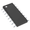 SN65LVDT32BDTexas InstrumentsIC RECEIVER 0/4 16SOIC
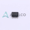 SN65LVDT2DRTexas InstrumentsIC RECEIVER 0/1 8SOIC
 SN65LVDT14PWRTexas InstrumentsIC TRANSCEIVER HALF 1/4 20TSSOP
 SN65LVDT2DG4Texas InstrumentsIC RECEIVER 0/1 8SOIC
 SN65LVDT14QPWREPTexas Instruments


