
 TLV5614IYZRTexas InstrumentsIC DAC 12BIT V-OUT 16WCSP
 TLV5616CPTexas InstrumentsIC DAC 12BIT V-OUT 8DIP
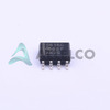 TLV5616CDRTexas InstrumentsIC DAC 12BIT V-OUT 8SOIC
 TLV5614IPWRTexas InstrumentsIC DAC 12BIT V-OUT 16TSSOP
- Nath***rooks
- Jun 11, 2026
HomeProductsIntegrated Circuits (ICs)Data Acquisition - Digital to Analog Converters (DAC)TLV5616CDG4


Image may be representation.
See specifications for product details.
See specifications for product details.
- EXPRESS OPTION
- Payment method
TLV5616CDG4 - Texas Instruments
- Manufacturer Part Number
- TLV5616CDG4
- Manufacturer
- Texas Instruments
- Allelco Part Number
- 98D-TLV5616CDG4
- Warranty
- 1 Year Allelco Warranty - Find out more
- Stock Status:
- 13,918 pcs available, New & Original
- Parts Description
- IC DAC 12BIT V-OUT 8SOIC
- Package
- 8-SOIC
- Data sheet
-
TLV5616CDG4.pdf
HTML Datasheet
TLV5616C, TLV5616I.pdf
- RoHs Status
- ROHS3 Compliant
- Our certification
- In stock: 13918
- Unit Price: $9.846
- Subtotal: $0.00
Want a better price?
Add to Cart and Submit RFQ now, we'll contact you immediately.
| Quantity | Unit Price | Ext. Price |
|---|---|---|
| 1+ | $9.846 | $9.85 |
| 200+ | $3.81 | $762.00 |
| 500+ | $3.677 | $1,838.50 |
| 1000+ | $3.61 | $3,610.00 |
The above prices does not include taxes and freight rates, which will be calculated on the order pages.


