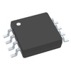

TLV5616CDGK (1)
Manufacturer Part Number
TLV5616CDGK
Manufacturer
Texas Instruments
Introduction
The TLV5616CDGK is a 12-bit digital-to-analog converter (DAC) designed for easy interfacing to microcontrollers.
Product Features and Performance
12-bit resolution
One D/A converter channel
20µs settling time
Buffered voltage output
SPI data interface
External reference voltage
Dual supply voltage support for analog and digital circuits
String DAC architecture
Industrial operating temperature range from 0°C to 70°C
Product Advantages
Low power consumption
High integration level with built-in output amplifier
Simple SPI interface for digital communications
Competitive accuracy with INL/DNL of ±1.9LSB and ±0.5LSB
Supports a wide range of supply voltages for flexible design options
Key Technical Parameters
Number of Bits: 12
Settling Time: 20µs
Output Type: Voltage - Buffered
Reference Type: External
Voltage - Supply, Analog: 2.7V ~ 3.3V, 5V
Voltage - Supply, Digital: 2.7V ~ 3.3V, 5V
INL/DNL (LSB): ±1.9, ±0.5
Operating Temperature: 0°C ~ 70°C
Quality and Safety Features
Precise calibration ensures accuracy
Robust design capable of operating in commercial temperature ranges
Compatibility
SPI interface compatible with many microcontrollers
Application Areas
Data acquisition systems
Process control
Instrumentation
Medical equipment
Battery-operated devices
Product Lifecycle
Active status
Not currently nearing discontinuation
Replacement or upgrade options may be available
Several Key Reasons to Choose This Product
High resolution of 12-bits tailored for precision applications
Fast settling time suitable for real-time data processing
Low-integral and differential nonlinearity errors enhance the accuracy of output signals
Flexible operation with multiple supply voltage options cater to diverse power requirements
The compact 8-VSSOP package enables miniaturization of PCB designs
Surface mount compatible for modern automated PCB assembly processes
Direct interfacing with a variety of microcontrollers facilitates ease of integration into existing systems

 TLV5614IYERTexas InstrumentsIC DAC 12BIT V-OUT 16WCSP
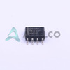 TLV5616CDRTexas InstrumentsIC DAC 12BIT V-OUT 8SOIC
 TLV5616CPTexas InstrumentsIC DAC 12BIT V-OUT 8DIP
 TLV5614MPWREPTexas Instruments


