 TMUX1108PWRTexas InstrumentsIC MUX 8:1 4OHM 16TSSOP
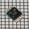 TMUX1121DGKRTexas InstrumentsIC SWITCH SPST X 2 4OHM 8VSSOP
 TMUX1119DBVRTexas InstrumentsIC SWITCH DPST X 1 4OHM SOT23-6
 TMUX1109RSVRTexas InstrumentsIC MUX DUAL 4:1 4OHM 16UQFN
 TMUX1119DCKRTexas InstrumentsIC SWITCH SPDT X 1 4OHM SC70-6
 TMUX1123DGKRTexas InstrumentsIC SWITCH SPST X 2 4OHM 8VSSOP
 TMUX1136DGSRTexas InstrumentsIC SWITCH SPDT X 2 4OHM 10VSSOP
 TMUX1113RSVRTexas InstrumentsIC SWITCH SPST X 4 4OHM 16UQFN
 TMUX1104DQARTexas InstrumentsIC SWITCH SP4T X 1 4OHM 10USON
 TMUX1111RSVRTexas Instruments
- Nath***rooks
- Jun 11, 2026
HomeProductsIntegrated Circuits (ICs)Interface - Analog Switches, Multiplexers, DemultiplexersTMUX1113PWR
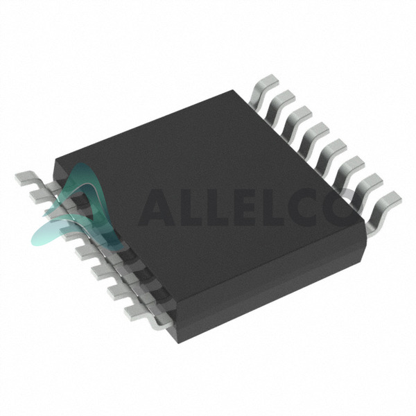
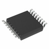
Image may be representation.
See specifications for product details.
See specifications for product details.
- EXPRESS OPTION
- Payment method
TMUX1113PWR - Texas Instruments
- Manufacturer Part Number
- TMUX1113PWR
- Manufacturer
- Texas Instruments
- Allelco Part Number
- 98D-TMUX1113PWR
- Warranty
- 1 Year Allelco Warranty - Find out more
- Stock Status:
- 45,042 pcs available, New & Original
- Parts Description
- IC SWITCH SPST X 4 4OHM 16TSSOP
- Package
- 16-TSSOP
- Data sheet
-
TMUX1113PWR.pdf
HTML Datasheet
TMUX111x Datasheet.pdf
- RoHs Status
- ROHS3 Compliant
- Our certification
- In stock: 45042
- Unit Price: $2.836
- Subtotal: $0.00
Want a better price?
Add to Cart and Submit RFQ now, we'll contact you immediately.
| Quantity | Unit Price | Ext. Price |
|---|---|---|
| 1+ | $2.836 | $2.84 |
| 10+ | $2.471 | $24.71 |
| 30+ | $2.253 | $67.59 |
| 100+ | $2.033 | $203.30 |
| 500+ | $1.932 | $966.00 |
| 1000+ | $1.886 | $1,886.00 |
The above prices does not include taxes and freight rates, which will be calculated on the order pages.


