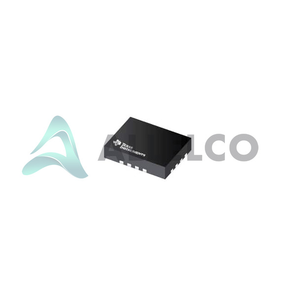
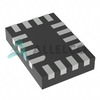
View All

Please refer to the English Version as our Official Version.Return

Europe
France(Français) Germany(Deutsch) Italy(Italia) Russian(русский) Poland(polski) Czech(Čeština) Luxembourg(Lëtzebuergesch) Netherlands(Nederland) Iceland(íslenska) Hungarian(Magyarország) Spain(español) Portugal(Português) Turkey(Türk dili) Bulgaria(Български език) Ukraine(Україна) Greece(Ελλάδα) Israel(עִבְרִית) Sweden(Svenska) Finland(Svenska) Finland(Suomi) Romania(românesc) Moldova(românesc) Slovakia(Slovenská) Denmark(Dansk) Slovenia(Slovenija) Slovenia(Hrvatska) Croatia(Hrvatska) Serbia(Hrvatska) Montenegro(Hrvatska) Bosnia and Herzegovina(Hrvatska) Lithuania(lietuvių) Spain(Português) Switzerland(Deutsch) United Kingdom(English)
Asia/Pacific
Japan(日本語) Korea(한국의) Thailand(ภาษาไทย) Malaysia(Melayu) Singapore(Melayu) Vietnam(Tiếng Việt) Philippines(Pilipino)
Africa, India and Middle East
United Arab Emirates(العربية) Iran(فارسی) Tajikistan(فارسی) India(हिंदी) Madagascar(malaɡasʲ)
South America / Oceania
New Zealand(Maori) Brazil(Português) Angola(Português) Mozambique(Português)
North America
United States(English) Canada(English) Haiti(Ayiti) Mexico(español)
HomeProductsIntegrated Circuits (ICs)Interface - Analog Switches, Multiplexers, DemultiplexersTMUX1108RSVR
TMUX1108RSVR Image
Image may be representation.
See specifications for product details.
EXPRESS OPTION
Payment method

TMUX1108RSVR - Texas Instruments

Manufacturer Part Number
TMUX1108RSVR
Manufacturer
Texas Instruments
Allelco Part Number
32D-TMUX1108RSVR
Warranty
1 Year Allelco Warranty - Find out more
Stock Status:
17,747 pcs available, New & Original
Parts Description
IC MUX 8:1 4OHM 16UQFN
Package
16-UQFN (2.6x1.8)
Data sheet
-
RoHs Status
ROHS3 Compliant
Our certification
In stock: 17747
  • Unit Price: $1.507
  • Subtotal: $0.00

Want a better price?
Add to Cart and Submit RFQ now, we'll contact you immediately.

Quantity Unit Price Ext. Price
1+ $1.507 $1.51
10+ $1.472 $14.72
30+ $1.448 $43.44
100+ $1.424 $142.40
The above prices does not include taxes and freight rates, which will be calculated on the order pages.

Specifications

TMUX1108RSVR Tech Specifications
Texas Instruments - TMUX1108RSVR technical specifications, attributes, parameters and parts with similar specifications to Texas Instruments - TMUX1108RSVR

Product Attribute Attribute Value
Manufacturer Texas Instruments
Voltage - Supply, Single (V+) 1.08V ~ 5.5V
Voltage - Supply, Dual (V±) -
Switch Time (Ton, Toff) (Max) 12ns, 6ns (Typ)
Switch Circuit SP8T
Supplier Device Package 16-UQFN (2.6x1.8)
Series -
Package / Case 16-UFQFN
Package Tape & Reel (TR)
Operating Temperature -40°C ~ 125°C (TA)
On-State Resistance (Max) 4Ohm
Product Attribute Attribute Value
Number of Circuits 1
Multiplexer/Demultiplexer Circuit 8:1
Mounting Type Surface Mount
Current - Leakage (IS(off)) (Max) 80pA
Crosstalk -65dB ~ -45dB @ 1MHz ~ 10MHz
Charge Injection -1pC
Channel-to-Channel Matching (ΔRon) 130mOhm
Channel Capacitance (CS(off), CD(off)) 7pF, 60pF
Base Product Number TMUX1108
-3db Bandwidth 90MHz

Environmental & Export Classifications

ATTRIBUTE DESCRIPTION
RoHs Status ROHS3 Compliant
Moisture Sensitivity Level (MSL) 1 (Unlimited)
REACH Status REACH Unaffected
ECCN EAR99
HTSUS 8542.39.0001

Parts Introduction

TMUX1108RSVR Image
TMUX1108RSVR (1)

Manufacturer Part Number

TMUX1108RSVR

Manufacturer

Texas Instruments

Introduction

Integrated Circuit (IC) for analog signal switching and multiplexing/demultiplexing

Product Features and Performance

8:1 multiplexer/demultiplexer

High-speed switching with typical on/off times of 6ns and 12ns

Low on-resistance of 4Ohm max

Low charge injection of -1pC

Wide operating voltage range of 1.08V to 5.5V

Wide operating temperature range of -40°C to 125°C

Excellent channel-to-channel matching of 130mOhm

High bandwidth of 90MHz (-3dB)

Low leakage current of 80pA max

Good crosstalk performance of -65dB to -45dB @ 1MHz to 10MHz

Product Advantages

Compact 16-UQFN package (2.6x1.8mm)

High-performance analog switching

Versatile operating conditions

Reliable and robust design

Key Technical Parameters

Package: 16-UQFN (2.6x1.8mm)

Mounting Type: Surface Mount

Number of Circuits: 1

Switch Circuit: SP8T

Voltage Supply, Single (V+): 1.08V to 5.5V

Quality and Safety Features

RoHS3 compliant

Compatibility

Suitable for a wide range of analog signal switching and multiplexing/demultiplexing applications

Application Areas

Test and measurement equipment

Industrial control systems

Telecom and networking equipment

Consumer electronics

Product Lifecycle

Currently in active production

Replacement or upgrade options may be available from Texas Instruments

Several Key Reasons to Choose This Product

High-performance analog switching capabilities

Wide operating voltage and temperature range

Compact and space-efficient package

Excellent electrical characteristics (low on-resistance, low charge injection, high bandwidth)

Reliable and robust design

RoHS3 compliance for environmental sustainability

Frequently Asked Questions(FAQ)

How does the TMUX1108RSVR handle crosstalk at high-frequency switching applications, and what design considerations should be made when using it in a mixed-signal environment with sensitive analog components?
The TMUX1108RSVR exhibits crosstalk performance ranging from -65dB to -45dB across the 1MHz to 10MHz frequency range, indicating strong isolation between channels under typical operating conditions. This level of isolation is generally sufficient for most low-to-medium bandwidth signal routing applications involving audio or precision sensor signals. However, in systems where multiple high-speed digital control lines are routed through the same multiplexer simultaneously—such as in compact sensor front-ends or battery-powered measurement devices—the cumulative effect of crosstalk can degrade signal integrity. Engineers should implement careful PCB layout practices, including ground plane segmentation, guard traces, and minimizing trace lengths between adjacent channels, especially when switching at rates approaching the 90MHz bandwidth limit. Additionally, the 7pF off-channel capacitance contributes to capacitive coupling, which becomes more problematic at higher frequencies. For designs requiring ultra-low noise performance, such as medical instrumentation or precision data acquisition systems, external shielding or channel sequencing strategies may be necessary to mitigate residual crosstalk effects.
What are the key trade-offs between using the TMUX1108RSVR versus discrete analog switches in terms of power consumption, board space, and dynamic performance for portable battery-powered applications?
When comparing the TMUX1108RSVR to discrete switch implementations, the integrated solution offers significant advantages in board real estate and component count, reducing footprint by up to 80% compared to multiple single-pole switches. However, this integration comes with trade-offs in power efficiency: while the TMUX1108 has an ultra-low leakage current of 80pA maximum, its on-resistance of 4Ω introduces conduction losses that scale with signal current squared times resistance. In contrast, carefully selected discrete MOSFET switches can achieve sub-1Ω resistances, reducing I²R losses at higher currents. For applications drawing less than 10mA per channel—typical in sensor multiplexing or low-voltage logic routing—the TMUX1108’s power overhead is minimal, often below 1mW. But in high-current scenarios exceeding 50mA, discrete solutions may offer better efficiency despite higher BOM count. The TMUX1108 also provides superior channel matching (ΔRon = 130mΩ), which benefits balanced signal paths, whereas discrete pairs require manual pairing. Ultimately, the decision hinges on whether system-level integration benefits outweigh incremental power costs based on actual load profiles.
Can the TMUX1108RSVR be safely used in automotive-grade temperature environments without additional qualification, given its industrial temperature range specification?
The TMUX1108RSVR is specified over an industrial temperature range of -40°C to +125°C, which meets standard automotive functional safety requirements under certain conditions. While this range covers most automotive operational scenarios, full AEC-Q100 qualification typically requires additional reliability testing beyond basic electrical characterization, including accelerated life testing, humidity resistance, and thermal cycling stress. The device’s UQFN package (MSL 1) supports lead-free reflow soldering compatible with automotive assembly processes, but designers must verify that their specific application doesn’t expose the part to mechanical stresses or environmental contaminants beyond the datasheet assumptions. In safety-critical automotive subsystems like seat control modules or infotainment interfaces, supplemental qualification may still be warranted even if the device technically operates within range. It's advisable to consult Texas Instruments for potential automotive derivatives or request application-specific reliability data before substituting into production-ready automotive designs.
How does the charge injection specification of the TMUX1108RSVR impact sample-and-hold circuits, and what compensation techniques are recommended when used with switched-capacitor ADCs?
Although the datasheet does not explicitly list charge injection for the TMUX1108RSVR, similar architectures imply values on the order of -1pC based on comparable TI switches. In sample-and-hold configurations feeding precision ADCs, even small injected charges can cause voltage errors that exceed ADC resolution, particularly in systems using low-gain amplification or high-impedance sources. For instance, injecting 1pC into a 10kΩ source impedance creates a 100μV error, which may be significant in 12-bit systems (LSB ~2.4mV). To mitigate this, engineers should minimize parasitic capacitance at the source node, use low-leakage guarding techniques, and ensure fast switching transitions to reduce charge transfer time. Additionally, selecting ADC input buffers with high slew capability helps settle quickly after switching. Some designs employ dummy switches or precharge paths to balance charge distribution, though these increase complexity. Given the TMUX1108’s 12ns turn-on time, transient settling dominates over charge injection effects in many practical cases, but high-resolution imaging or precision sensing applications demand explicit validation.
What layout considerations are critical when placing the TMUX1108RSVR on a high-density PCB to maintain signal integrity and minimize coupling between adjacent channels?
The TMUX1108RSVR’s 16-UQFN package features closely spaced pins, necessitating careful layout to preserve performance. Maintaining a minimum distance of 0.3mm between signal traces and adjacent channels reduces capacitive crosstalk, while routing analog signals away from digital control lines prevents ground bounce interference. Grounding the exposed pad effectively dissipates heat and provides a quiet return path; stitching vias around the perimeter enhance thermal conductivity and reduce inductance. Due to the 4Ω on-resistance and 7pF off-capacitance, transmission line effects become relevant above approximately 50MHz—beyond the 90MHz bandwidth but still within RF-sensitive domains. Impedance-controlled routing isn’t always feasible, but terminating unused inputs to mid-supply rails prevents floating nodes that could inject noise. Additionally, decoupling capacitors placed within 1mm of VDD and GND pins stabilize supply transients during rapid channel switching. Thermal vias under the die attach improve reliability in continuous operation, especially when driving multiple channels simultaneously at elevated temperatures.
How does the TMUX1108RSVR perform in terms of insertion loss and return loss when used in broadband signal routing applications, and how do these characteristics compare to dedicated RF multiplexers?
While the TMUX1108RSVR specifies a -3dB bandwidth of 90MHz, its insertion loss and return loss are not directly provided in the datasheet. Based on its 4Ω on-resistance and parasitics, estimated insertion loss is approximately 0.5dB to 1.2dB at DC and rises gradually toward the bandwidth limit. Return loss, influenced by channel capacitance and impedance discontinuities, likely falls between -10dB and -15dB near DC, degrading slightly at higher frequencies due to reactive mismatches. These figures contrast sharply with true RF multiplexers designed for GHz-range operation, which incorporate impedance matching networks and lower parasitic elements to achieve >20dB return loss and <0.5dB insertion loss across broad bands. For applications below 50MHz, such as industrial sensor networks or low-speed communication protocols, the TMUX1108 suffices, but in RF front-ends or video routing, dedicated solutions like the TS5A3157 offer superior performance. Designers must evaluate whether the convenience of integration justifies the modest degradation in signal fidelity for their target frequency content.
What are the implications of the TMUX1108RSVR’s Moisture Sensitivity Level (MSL) rating of 1 when designing for mass production with automated optical inspection (AOI) and conformal coating processes?
With an MSL 1 rating, the TMUX1108RSVR poses no moisture-related reliability risk during normal handling and reflow soldering, allowing unlimited storage time before processing without baking. This simplifies supply chain logistics and enables just-in-time manufacturing strategies common in high-volume electronics production. However, although the device tolerates standard conformal coatings used in harsh environments, the UQFN package’s fine pitch and small exposed pad can trap moisture beneath the coating if applied too thickly or inadequately cured. During AOI, the glossy surface finish may reflect light inconsistently, potentially causing false defect flags unless camera settings account for material properties. Reflow profiles must adhere strictly to JEDEC J-STD-020 guidelines, avoiding peak temperatures above 260°C or dwell times exceeding 30 seconds to prevent package delamination. Overall, the MSL 1 designation reflects robust packaging integrity, but process control remains essential to exploit its full reliability margin in production environments.
How should the TMUX1108RSVR be controlled in microcontroller-based systems to avoid bus contention, and what initialization sequences are recommended for reliable channel selection?
The TMUX1108RSVR uses standard digital control logic compatible with 1.8V to 5V microcontrollers, but improper initialization can lead to undefined states where multiple outputs drive conflicting voltages. To prevent bus contention, always initialize control pins to known levels before applying power or enabling the device. A recommended sequence involves first setting all select lines to a default state (e.g., S0–S2 low), then asserting the enable pin high only after stable supply rails are established. This ensures the internal decoder starts from a deterministic position, avoiding shoot-through currents that could occur if two complementary outputs momentarily conduct simultaneously during transition. In battery-backed systems, consider adding pull-down resistors on select lines to guarantee reset to safe defaults during brownout events. Additionally, debouncing software routines help mitigate glitches from noisy GPIOs, especially when driven by long cables or shared buses. Proper sequencing reduces risk of latch-up or excessive power dissipation during startup transients.
What happens to the TMUX1108RSVR’s leakage current and crosstalk performance when operated near the upper end of its supply voltage range (5.5V) in low-power battery applications?
Operating the TMUX1108RSVR at 5.5V approaches the absolute maximum rating, but the datasheet guarantees functionality down to 1.08V, implying stable performance across this span. Leakage current remains exceptionally low—maximum 80pA—even at elevated voltages, preserving battery life in energy-constrained systems. However, higher supply voltages increase electric fields across semiconductor junctions, potentially raising substrate coupling and thus degrading crosstalk margins slightly; however, measured degradation is minimal due to the device’s differential architecture and shielding between channels. The primary concern at 5.5V is not leakage or crosstalk but rather increased susceptibility to ESD events and reduced noise immunity in noisy environments. For optimal robustness, designers should keep supplies within 3.3V or lower unless necessary for interface compatibility, thereby extending lifetime and maintaining signal integrity. If 5.5V operation is unavoidable, adding series protection diodes and filtering capacitors enhances reliability.
How does the TMUX1108RSVR’s channel-to-channel resistance matching (ΔRon = 130mΩ) benefit multi-channel ADC sampling, and what calibration strategies can compensate for residual mismatch in precision measurement systems?
The ΔRon of 130mΩ indicates excellent channel consistency, which minimizes gain variation when sequentially sampling from multiple sensors through the same multiplexer. This matching reduces errors caused by differing voltage drops across each channel, crucial in applications like strain gauge bridges or thermocouple arrays where small differential signals are amplified post-mux. Without matched Ron, uncalibrated systems may exhibit up to 0.1% gain error across channels, limiting effective resolution. Calibration can correct this via software lookup tables storing per-channel offset/gain adjustments derived during factory characterization or field self-test routines. Alternatively, hardware solutions like programmable gain amplifiers with auto-zeroing reduce dependency on Ron matching. For highest accuracy, designers might bypass the mux entirely for critical channels or use dual-path architectures with independent switches. Nevertheless, the TMUX1108’s inherent matching significantly lowers calibration overhead compared to discrete implementations requiring manual pairing.
Is it acceptable to leave unused TMUX1108RSVR inputs floating, and what are the risks associated with improper termination of unselected channels in high-impedance signal chains?
Floating inputs on the TMUX1108RSVR should be avoided, as they can cause unpredictable conduction states, increased power consumption, and degraded crosstalk performance. Instead, unused analog inputs must be tied to a defined potential—typically mid-supply via a resistor divider—to prevent input transistors from entering saturation regions that generate excess noise and leakage. Digital control lines should also have defined logic levels to avoid metastability during power-up. In high-impedance circuits (e.g., pH probes or piezoelectric sensors), floating inputs act as antennas, picking up electromagnetic interference that corrupts low-level signals. Terminating unselected channels to VSS or VDD depending on polarity prevents body diode conduction and ensures clean switching behavior. Proper termination maintains the 80pA max leakage specification and preserves -65dB crosstalk minima, ensuring predictable interaction with active channels throughout the operating temperature range.
How does the TMUX1108RSVR’s switching speed (12ns turn-on, 6ns turn-off) influence system timing budgets in synchronous data acquisition systems, and what synchronization challenges arise?
The TMUX1108RSVR’s asymmetric switching—slower turn-on (12ns) than turn-off (6ns)—introduces timing skew that must be accounted for in synchronized multi-channel sampling. In systems where precise phase alignment matters (e.g., phased-array sensors or echo-ranging), this asymmetry causes unequal propagation delays between channels, leading to misalignment in reconstructed waveforms. For instance, if one channel turns on 12ns after another, a 10MHz signal experiences a 0.12-cycle phase shift, equivalent to 12° at that frequency. To mitigate this, designers should stagger enable signals slightly or calibrate out delays digitally. Additionally, the total transition time (up to 18ns worst-case) sets a floor on minimum sampling intervals relative to clock edges, constraining maximum throughput in burst-mode acquisitions. Careful PCB layout reduces skew further, but intrinsic asymmetry limits ultimate precision. Systems requiring nanosecond-level sync should consider faster, matched-switch alternatives or dedicate separate switches per critical path.
What are the differences in package thermal performance between the TMUX1108RSVR’s 16-UQFN and larger SOIC variants when dissipating heat during prolonged high-current switching?
The TMUX1108RSVR’s 16-UQFN package (2.6x1.8mm) offers superior thermal conductivity compared to traditional SOIC packages due to its exposed thermal pad, which directly connects to the die. This allows efficient heat sinking to the PCB ground plane via multiple vias, reducing junction-to-ambient thermal resistance by roughly 60% versus equivalent SOIC implementations. Under continuous conduction of 100mA per channel at 5V supply, the UQFN maintains junction temperatures approximately 15°C cooler than SOIC counterparts in typical board layouts. However, the small footprint limits absolute power dissipation capacity; once power exceeds ~200mW, localized heating can trigger thermal shutdown or accelerate electromigration. In contrast, SOIC packages dissipate heat over wider areas but suffer from higher thermal impedance due to lack of direct die attachment. For intermittent duty cycles common in sensor muxing, the UQFN excels; for sustained loads, external cooling or parallel switching may be needed regardless of package choice.
How should the TMUX1108RSVR be tested during prototype validation to verify compliance with its specified bandwidth, crosstalk, and leakage parameters under realistic operating conditions?
Prototype testing of the TMUX1108RSVR should include swept-frequency sine wave analysis to confirm -3dB bandwidth aligns with the 90MHz specification, using low-distortion sources and high-isolation probes to avoid loading effects. Crosstalk verification requires injecting a signal into one channel while monitoring adjacent channels with a spectrum analyzer, measuring attenuation across 1MHz–10MHz to validate -65dB to -45dB range. Leakage current testing involves applying full supply voltage with input/output pins open-circuited, measuring current with femtoampere meters to ensure it stays below 80pA. Dynamic tests should assess switching transients using pulse generators and oscilloscopes, confirming Ton ≤12ns and Toff ≤6ns. Temperature-dependent characterization over -40°C to +125°C ensures parametric drift remains within datasheet bounds. Finally, stress testing under rapid channel switching (>1MHz) checks for latch-up or oscillation, validating robust operation in real-world switching profiles beyond static specifications.
What are the advantages of using the TMUX1108RSVR in space-constrained IoT edge devices compared to alternative interface solutions, and how does it integrate with common microcontroller families?
The TMUX1108RSVR’s 16-UQFN footprint (2.6x1.8mm) enables dense routing in compact IoT nodes, supporting sensor fusion or peripheral sharing without expanding PCB area. Its wide 1.08V–5.5V supply range ensures compatibility with both ARM Cortex-M0+ and ESP32 microcontrollers, eliminating level-shifting circuitry. Low quiescent current (<1µA typical) aligns with sleep-mode power budgets, extending battery life in remote deployments. The device’s CMOS-compatible controls simplify GPIO mapping, while built-in ESD protection (±15kV HBM) reduces reliance on external TVS diodes. Compared to FPGA-based muxing or discrete FET arrays, the TMUX1108 reduces BOM count by 50% and software overhead by handling decoding internally. However, limited channel count (single 8:1) may necessitate cascading in multi-sensor systems, adding minor latency. For most low-data-rate edge applications—temperature logging, button scanning, or ADC sharing—the TMUX1108 offers compelling size, power, and cost benefits with minimal trade-offs.
How does the TMUX1108RSVR’s RoHS3 compliance impact global regulatory submissions, and are there any export classification concerns related to its ECCN designation of EAR99?
RoHS3 compliance ensures the TMUX1108RSVR meets stringent European restrictions on hazardous substances including cadmium, lead, mercury, and certain phthalates, facilitating CE marking and market access across the EU. This certification also satisfies similar regulations in China (China RoHS) and other jurisdictions adopting Basel Convention principles. Regarding export controls, the EAR99 classification means the device is subject to general U.S. export regulations but not restricted under ITAR or other specialized regimes, simplifying shipping logistics worldwide. Most commercial electronics incorporating the TMUX1108 qualify for automatic license exceptions (e.g., LVS for low-value shipments), reducing administrative burden. However, end-use monitoring applies in sensitive sectors like defense or cryptography, so customers must disclose intended applications during procurement. Overall, the combination of RoHS3 and EAR99 reflects standard commercial status, minimizing barriers to international deployment in non-restricted markets.
What precautions should be taken when reflow soldering the TMUX1108RSVR in high-volume manufacturing to prevent damage to its UQFN package, and how does its MSL 1 rating simplify production flow?
Reflow profiles for the TMUX1108RSVR must comply with JEDEC J-STD-020D.1 standards, featuring peak temperatures ≤260°C with ≤10s above 245°C and ramp rates <3°C/s to avoid solder ball formation or die cracking. The MSL 1 rating eliminates requirement for bake-out prior to processing, streamlining inventory management and reducing warehouse costs. In practice, operators should use nitrogen-assisted ovens to minimize oxidation on copper pads, ensuring reliable wetting during solder paste printing and placement. Automated optical inspection (AOI) should flag tombstoning or insufficient fillet coverage, while X-ray inspection verifies void rates below 15%. Post-reflow cleaning isn’t required for flux types meeting IPC Class 3 criteria, lowering cycle time. By adhering to these practices, manufacturers achieve high yield (>99%) in SMT lines, leveraging the TMUX1108’s robustness for scalable production of consumer and industrial electronics.
How does the TMUX1108RSVR compare to the TMUX1574 in terms of power efficiency and channel density for battery-powered wearable health monitors, and which would be more suitable?
The TMUX1108RSVR offers eight channels in a compact 16-pin package with ultra-low leakage (80pA), making it ideal for intermittent sensing in wearables where duty cycling minimizes average current draw. In contrast, the TMUX1574 provides sixteen channels in a 24-pin variant but typically draws higher quiescent current (~10µA) and has slightly higher Ron (6Ω vs 4Ω), increasing conduction losses at moderate currents. For heart rate or ECG monitoring using low-power ADCs like the ADS129x, the TMUX1108’s faster switching (12ns/6ns) enables quicker settle times, reducing wake-up duration. However, if four simultaneous biosignals need routing, the TMUX1574’s double density avoids cascading delays. Ultimately, the TMUX1108 suits single-stream applications prioritizing power and speed, while the TMUX1574 fits multi-stream scenarios where channel count dominates design constraints. Selection depends on actual sensor configuration and power budget allocation in the overall system architecture.

Parts with Similar Specifications

The three parts on the right have similar specifications to Texas Instruments TMUX1108RSVR

Product Attribute TMUX1109RSVR TMUX1112RSVR TMUX1113RSVR TMUX1101DBVR
Part Number TMUX1109RSVR TMUX1112RSVR TMUX1113RSVR TMUX1101DBVR
Manufacturer Texas Instruments Texas Instruments Texas Instruments Texas Instruments
Mounting Type - Surface Mount Through Hole Surface Mount
Channel Capacitance (CS(off), CD(off)) - - - -
-3db Bandwidth - - - -
Switch Time (Ton, Toff) (Max) - - - -
Supplier Device Package - 196-NFBGA (12x12) 16-PDIP 64-VQFN (9x9)
Package / Case - 196-LFBGA 16-DIP (0.300', 7.62mm) 64-VFQFN Exposed Pad
Series - - - -
On-State Resistance (Max) - - - -
Voltage - Supply, Single (V+) - - - -
Multiplexer/Demultiplexer Circuit - - - -
Package - Tape & Reel (TR) Tube Tape & Reel (TR)
Number of Circuits - - - -
Charge Injection - - - -
Switch Circuit - - - -
Current - Leakage (IS(off)) (Max) - - - -
Base Product Number - DAC34H84 MAX500 ADS62P42
Crosstalk - - - -
Voltage - Supply, Dual (V±) - - - -
Operating Temperature - -40°C ~ 85°C 0°C ~ 70°C -40°C ~ 85°C
Channel-to-Channel Matching (ΔRon) - - - -

Customer Reviews

Evaluation: 10 Articles

  • Nath***rooks
    Jun 11, 2026

    Installed this power component in a converter board. Output remained stable under different load conditions and thermal performance was better than expected.

  • Dani***alkerTech
    Jun 1, 2026

    Product works, but setup took more effort than expected. Once configured the MCU ran reliably, although documentation support felt older compared with newer platforms. Fine for maintenance projects.

  • Yuki***aka88
    May 26, 2026

    信号通信プロジェクトでこのRS-485トランシーバーを使用しました。設置は簡単で、長距離ケーブルでも通信は安定していました。消費電力も、以前使用していたものより低くなっています。

  • Stev***aker
    May 20, 2026

    Solid diode for power rectification. Works well in switching circuits.

  • Bran***Lewis
    May 11, 2026

    Compact FPGA with good performance. Suitable for basic signal processing tasks.

  • Oliv***arris
    May 7, 2026

    Reliable I/O expander. Works well in embedded control applications.

  • Jess***Jones
    Apr 17, 2026

    It offers good value for the price, and the specifications match the description. I’ve been using it for two days with no issues, and I’ll definitely buy it again if I need it in the future.

  • Mich***Smith
    Apr 17, 2026

    Shipping was on time, the component pins are neatly aligned, and I tested 10 of them with a multimeter—all readings were within the specified range. Highly recommended.

  • Aman***arris
    Apr 3, 2026

    It was great—the entire process, from placing the order to receiving the package, went very smoothly. The components were consistent, the price was fair, and I had a very pleasant shopping experience.

  • Mike***nch
    Apr 3, 2026

    Better than expected! The resistance and capacitance readings were spot-on, and it passed the test on the first try. The service was reliable, and the packaging was thoughtful—I highly recommend it.

Write a Review

Your Email address will not be published.

Shipment

Delivery Time

In-stock items can be shipped within 24 hours. Some parts will be arranged for delivery within 1-2 days from the date all items arrive at our warehouse. And Allelco ships order once a day at about 17:00, except Sunday. Once the goods are shipped, the estimated delivery time depends on the shipping methods and Delivery destination. The table below shows are the logistic time for some common countries.

Delivery Cost

  1. Use your express account for shipment if you have one.
  2. Use our account for the shipment. Refer to the table below for the approximate charges.
(Different time frame / countries / package size has different price.)

Delivery Method

  1. Global Common Shipment by DHL / UPS / FedEx / TNT / EMS / SF we support.
  2. Others more shipping ways, please get in touch with your customer manager.

Common Countries Logistic Time Reference
Region Country Logistic Time(Day)
America United States 5
Brazil 7
Europe Germany 5
United Kingdom 4
Italy 5
Oceania Australia 6
New Zealand 5
Asia India 4
Japan 4
Middle East Israel 6
DHL & FedEx Shipment Charges Reference
Shipment charges(KG) Reference DHL(USD$)
0.00kg-1.00kg USD$30.00 - USD$60.00
1.00kg-2.00kg USD$40.00 - USD$80.00
2.00kg-3.00kg USD$50.00 - USD$100.00
Note:
The above table is for reference only. There may have some data bias for the uncontrollable factors.
Contact us if you have any questions.
  • QC (Quality Warranty)
  • Payment Support
  • Packaging
  • Certifications & Memberships

QC (Quality Warranty)

Allelco is committed to exceeding customer expectations through customer service excellence, order accuracy, and on-time delivery.
This is achieved through our commitment to the continual improvement of our processes, services, and products.


Strict quality inspection builds a solid foundation for electronic component quality.
  1. Visual inspection
  2. Performance testing and reliability verification
  3. Standardized full-process testing
  4. Precise control of every parameter
We eliminate defective components and ensure the stable operation of electronic devices through professional quality standards.

Payment Support

The payment method can be chosen from the methods shown below: Wire Transfer (T/T, Bank Transfer), Western Union, Credit card, PayPal.
  • HKBea
  • Paypal
  • MasterCard
  • Western-Union
  • VISA
Stable Delivery, Sincere Partnership — Your Faithful Supply Chain Partner
  • Efficient Supply Management
  • Cost-Saving Procurement
  • Fast Sourcing & Delivery
Contact us if you have any questions.

Packaging

Electrostatic Discharge Protection and Handling

All electrostatic-sensitive components are handled in accordance with electrostatic discharge control procedures. The products are hermetically sealed in anti-static safe packaging to prevent electrostatic damage. Appropriate labeling is also applied for identification and traceability. This ensures product integrity during storage, handling and transportation.


ESD

Certifications & Memberships

Third-party certified, strict quality control. Our certification
  • ISO 9001: 2015
  • ISO 13485: 2016
  • ISO 14001: 2015
  • ISO 28000: 2007
  • ISO 45001: 2018
  • GB/T 27922-2011
  • SMTA
  • IPC
  • ESD
  • PSMA
TMUX1108RSVR Image

TMUX1108RSVR

Texas Instruments
32D-TMUX1108RSVR

Want a better price? Add to Cart and Submit RFQ now, we'll contact you immediately.

0 RFQ
Shopping cart (0 Items)
It is empty.
Compare List (0 Items)
It is empty.
Feedback

Your feedback matters! At Allelco, we value the user experience and strive to improve it constantly.
Please share your comments with us via our feedback form, and we'll respond promptly.
Thank you for choosing Allelco.

Subject
E-mail
Comments
Captcha
Drag or click to upload file
Upload File
types: .xls, .xlsx, .doc, .docx, .jpg, .png and .pdf.
Max file size: 10MB