View All

Please refer to the English Version as our Official Version.Return

Europe
France(Français) Germany(Deutsch) Italy(Italia) Russian(русский) Poland(polski) Czech(Čeština) Luxembourg(Lëtzebuergesch) Netherlands(Nederland) Iceland(íslenska) Hungarian(Magyarország) Spain(español) Portugal(Português) Turkey(Türk dili) Bulgaria(Български език) Ukraine(Україна) Greece(Ελλάδα) Israel(עִבְרִית) Sweden(Svenska) Finland(Svenska) Finland(Suomi) Romania(românesc) Moldova(românesc) Slovakia(Slovenská) Denmark(Dansk) Slovenia(Slovenija) Slovenia(Hrvatska) Croatia(Hrvatska) Serbia(Hrvatska) Montenegro(Hrvatska) Bosnia and Herzegovina(Hrvatska) Lithuania(lietuvių) Spain(Português) Switzerland(Deutsch) United Kingdom(English)
Asia/Pacific
Japan(日本語) Korea(한국의) Thailand(ภาษาไทย) Malaysia(Melayu) Singapore(Melayu) Vietnam(Tiếng Việt) Philippines(Pilipino)
Africa, India and Middle East
United Arab Emirates(العربية) Iran(فارسی) Tajikistan(فارسی) India(हिंदी) Madagascar(malaɡasʲ)
South America / Oceania
New Zealand(Maori) Brazil(Português) Angola(Português) Mozambique(Português)
North America
United States(English) Canada(English) Haiti(Ayiti) Mexico(español)
HomeProductsIntegrated Circuits (ICs)Embedded - MicrocontrollersMSP430F5249IZQER
MSP430F5249IZQER Image
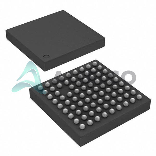
Image may be representation.
See specifications for product details.
EXPRESS OPTION
Payment method

MSP430F5249IZQER - Texas Instruments

Manufacturer Part Number
MSP430F5249IZQER
Manufacturer
Texas Instruments
Allelco Part Number
98D-MSP430F5249IZQER
Warranty
1 Year Allelco Warranty - Find out more
Stock Status:
6,846 pcs available, New & Original
Parts Description
IC MCU 16BIT 128KB FLASH 80BGA
Package
80-BGA MICROSTAR JUNIOR (5x5)
Data sheet
MSP430F5249IZQE.pdf
RoHs Status
ROHS3 Compliant
Our certification
In stock: 6846

Required fields are indicated by an asterisk (*)
Please send RFQ, we will respond immediately.

Quantity

Specifications

MSP430F5249IZQER Tech Specifications
Texas Instruments - MSP430F5249IZQER technical specifications, attributes, parameters and parts with similar specifications to Texas Instruments - MSP430F5249IZQER

Product Attribute Attribute Value
Manufacturer Texas Instruments
Voltage - Supply (Vcc/Vdd) 1.8V ~ 3.6V
Supplier Device Package 80-BGA MICROSTAR JUNIOR (5x5)
Speed 25MHz
Series MSP430F5xx
RAM Size 8K x 8
Program Memory Type FLASH
Program Memory Size 128KB (128K x 8)
Peripherals Brown-out Detect/Reset, DMA, POR, PWM, WDT
Package / Case 80-VFBGA
Package Tape & Reel (TR)
Product Attribute Attribute Value
Oscillator Type Internal
Operating Temperature -40°C ~ 85°C (TA)
Number of I/O 53
Mounting Type Surface Mount
EEPROM Size -
Data Converters A/D 12x10b
Core Size 16-Bit
Core Processor MSP430 CPUXV2
Connectivity I²C, IrDA, SPI, UART/USART
Base Product Number MSP430F5249

Environmental & Export Classifications

ATTRIBUTE DESCRIPTION
RoHs Status ROHS3 Compliant
Moisture Sensitivity Level (MSL) 3 (168 Hours)
REACH Status REACH Unaffected
ECCN EAR99
HTSUS 8542.31.0001

Frequently Asked Questions(FAQ)

What are the key performance trade-offs when selecting the MSP430F5249IZQER for a low-power embedded system with real-time sensor data acquisition?
The MSP430F5249IZQER offers a balanced architecture suitable for energy-constrained applications, but designers must consider its 8KB RAM limitation when handling large sensor datasets. While its 25MHz clock speed and 128KB FLASH support efficient data processing, the lack of integrated EEPROM means non-volatile parameter storage requires external solutions or FLASH wear-leveling algorithms. Its 12-channel, 10-bit ADC enables precise analog measurements, but higher resolution or faster sampling may require external converters. The device’s ultra-low active power consumption (as low as 160µA/MHz) is offset by longer wake-up times from sleep modes, impacting responsiveness in time-critical tasks.
How does the MSP430F5249IZQER compare to the MSP430F5249IRGCR in terms of thermal performance and PCB layout complexity?
The MSP430F5249IZQER uses an 80-BGA MICROSTAR JUNIOR (5x5) package with a smaller footprint than the IRGCR’s 80-VQFN, offering better space efficiency but demanding significantly tighter PCB design tolerances. BGA assembly requires advanced soldering techniques and X-ray inspection due to its 0.4mm pitch. In contrast, the VQFN version allows for more forgiving surface-mount processes. Both share identical electrical characteristics, but the BGA package has slightly higher thermal resistance due to reduced copper exposure, potentially requiring careful thermal via placement under the exposed pad during board layout to maintain junction temperatures below 85°C under full load.
Can the MSP430F5249IZQER be used in automotive-grade temperature monitoring systems, and what design precautions are necessary?
The MSP430F5249IZQER operates reliably from -40°C to +85°C, which covers most industrial and commercial temperature ranges, including many automotive environments. However, it is not AEC-Q100 qualified, so its use in safety-critical automotive applications should be carefully evaluated. Designers must ensure proper decoupling near the Vcc pins, use stable external references if high ADC accuracy is needed, and implement watchdog and brown-out reset circuits to handle power fluctuations. Additionally, signal integrity on high-speed interfaces like SPI or I2C should be maintained through controlled impedance routing and shielding where required.
What is the impact of using internal versus external oscillators with the MSP430F5249IZQER, particularly in battery-powered devices?
The MSP430F5249IZQER includes an internal 25MHz DCO oscillator that can be trimmed for accuracy but typically has ±1% tolerance. For precision timing or communication protocols like UART at high baud rates, this variation may exceed acceptable limits. Using an external crystal improves stability and reduces calibration overhead, saving FLASH memory used for trimming codes. However, crystals consume more power and add cost and board space. In low-power designs, the device’s flexible clock system allows switching between internal and external sources, enabling duty-cycled operation where the MCU runs briefly with the crystal for accurate transmission before reverting to the low-power internal oscillator.
How does the 80-BGA packaging affect the reliability of the MSP430F5249IZQER in harsh mechanical environments?
The 80-BGA MICROSTAR JUNIOR (5x5) package provides excellent electrical performance and compact size but presents mechanical challenges under vibration and thermal cycling. BGA solder joints are prone to fatigue failure if subjected to repeated stress. To enhance reliability, designers should avoid placing the IC near edges of PCBs, use stiffeners, and minimize layer transitions near the BGA. Thermal management is critical—ensuring adequate heat dissipation through vias under the die helps prevent warpage and solder joint cracking. MSL level 3 indicates standard moisture sensitivity, but reflow profiles must comply with IPC standards to avoid popcorning during assembly.
What are the limitations of the MSP430F5249IZQER’s PWM capabilities when driving motor control loads?
The MSP430F5249IZQER includes multiple PWM modules capable of generating up to 16 independent channels, but all share a maximum frequency of approximately 1 MHz with 10-bit resolution. This is sufficient for many servo and stepper motor applications but insufficient for high-frequency BLDC motor drives requiring >100kHz switching. Additionally, output drive strength is limited to standard CMOS levels (~3.3V, 8–12mA), necessitating external drivers for inductive loads. The lack of complementary outputs or dead-time generation in hardware limits H-bridge control without software intervention, increasing CPU load and potential for shoot-through faults.
Is the MSP430F5249IZQER suitable for firmware development with real-time operating systems (RTOS), and what constraints apply?
Yes, the MSP430F5249IZQER supports RTOS integration due to its 8KB RAM and deterministic interrupt response. However, task stacks and kernel overhead consume a significant portion of available RAM—typical RTOS usage may occupy 1–2KB, leaving limited headroom for application buffers and context switching. Developers must optimize ISR duration to avoid blocking other tasks and carefully manage shared resources. The built-in DMA controller offloads data transfers from the CPU, reducing latency and freeing cycles for RTOS scheduling. Careful partitioning of memory regions and use of static allocation rather than dynamic memory are recommended to ensure timing predictability.
How does the absence of on-chip EEPROM in the MSP430F5249IZQER affect system calibration and configuration persistence?
Unlike some MSP430 variants, the MSP430F5249IZQER lacks integrated EEPROM, so calibration coefficients, device-specific IDs, or user configurations cannot be stored non-volatily without external components. Designers often reserve a small section of FLASH (e.g., 512 bytes) for such data, implementing wear-leveling and periodic backup routines. This increases firmware complexity and risks corruption during power loss. Alternatively, external serial EEPROMs (like 24xx series) add cost and pins, but offer larger capacity and byte-wise write flexibility. The choice depends on update frequency, endurance requirements, and system cost targets.
What considerations apply when interfacing the MSP430F5249IZQER with 5V logic systems using its 3.3V I/O banks?
The MSP430F5249IZQER operates at 1.8V–3.6V, so direct connection to 5V logic (e.g., older sensors or legacy peripherals) risks damaging the MCU. Level shifting is mandatory. Simple resistor-divider networks suffice for unidirectional signals but do not protect against reverse voltage. Bidirectional interfaces require dedicated transceivers like TXB0104 or MOSFET-based level shifters. For UART/I2C, open-drain signaling allows safe 5V pull-ups only if input thresholds are compatible; otherwise, active translation is needed. Always verify voltage compliance across all pins, especially during power sequencing.
How does the DMA feature in the MSP430F5249IZQER improve system efficiency in data-intensive applications?
The MSP430F5249IZQER includes a DMA controller that transfers data between memory and peripherals without CPU intervention, reducing interrupt frequency and CPU load. For example, continuous ADC sampling into RAM can occur while the CPU sleeps, waking only after buffer thresholds are reached. This enables low-latency, high-throughput data capture essential for audio processing or sensor fusion. The DMA supports multiple channel priorities and burst modes, allowing flexible configuration. Proper buffer alignment and double-buffering techniques prevent data loss during transfers, maximizing effective throughput even at high sample rates.
What are the implications of the MSP430F5249IZQER’s Moisture Sensitivity Level (MSL) 3 classification for manufacturing and handling?
MSL 3 indicates the MSP430F5249IZQER can withstand up to 168 hours of exposure to ambient conditions before requiring baking. After opening the moisture barrier bag, the component must be assembled within this window unless baked per JEDEC J-STD-033. Failure to comply risks delamination and popcorn cracking during reflow. Facilities must track time-to-assembly and maintain controlled storage (dry cabinets with desiccant). This applies equally to prototype builds and mass production. Proper handling procedures, including ESD protection and humidity monitoring, are essential to preserve reliability throughout the supply chain.
Can the MSP430F5249IZQER replace microcontrollers with integrated CAN or LIN interfaces in automotive lighting control?
No, the MSP430F5249IZQER lacks native CAN or LIN transceivers, making it unsuitable for direct replacement in automotive networks requiring these protocols. While it supports UART/USART and can emulate LIN via bit-banging, this approach consumes CPU cycles and lacks hardware error detection. For automotive lighting, where timing and fault tolerance matter, dedicated transceivers like TJA1050 (CAN) or TJA1021 (LIN) are preferred. The MSP430F5249IZQER could still serve as a host processor behind such a transceiver, handling PWM generation and diagnostics, but not as a standalone node.
What are the best practices for minimizing power consumption in the MSP430F5249IZQER during standby operation?
To minimize power in the MSP430F5249IZQER, enable deep sleep mode (LPM3 or LPM4), disable unused clocks, turn off analog peripherals via control registers, and configure GPIOs as inputs with pull-downs to prevent leakage. Use the real-time clock (RTC) or external interrupts to wake the device periodically. The RTC draws less than 1µA in LPM3. Avoid leaving unused pins floating—they can cause parasitic current paths. Also, ensure supply rails are clean and bypass capacitors are placed close to VCC/GND pins to reduce switching noise that increases quiescent current.
How does the 128KB FLASH memory of the MSP430F5249IZQER constrain firmware updates and over-the-air (OTA) functionality?
The 128KB FLASH provides ample space for most embedded applications, but OTA updates require careful planning. Firmware must support partial image flashing and rollback mechanisms to survive failed updates. Since FLASH has limited erase/write cycles (~10k), frequent writes reduce longevity. Delta updates and compression help mitigate this. Additionally, the BGA package complicates debugging and recovery—if a corrupted flash renders the device unresponsive, programming may require specialized equipment. Secure boot and cryptographic verification become essential to prevent malicious updates, adding computational overhead that strains the 25MHz CPU.
What are the advantages of using the MSP430F5249IZQER in wearable health monitoring devices compared to general-purpose MCUs?
The MSP430F5249IZQER excels in wearables due to its ultra-low active and sleep currents, compact 5x5mm BGA package, and integrated precision ADC for bio-signal conditioning. Its wake-on-interrupt capability allows duty-cycling sensors like accelerometers or PPG LEDs, extending battery life. The 16-bit CPU efficiently handles digital filters and baseline wander removal in ECG signals. However, the limited RAM may restrict complex algorithms, requiring external SRAM or simplified processing. The absence of USB hardware (only UART/I2C/SPI) simplifies connectivity but limits direct PC interfacing without protocol conversion.
How does the operating voltage range of 1.8V–3.6V influence power supply design for the MSP430F5249IZQER?
The wide supply range offers flexibility but demands robust regulation. Buck-boost converters or LDOs with low dropout (e.g., <100mV at 3.3V) are common choices. At 1.8V, noise margins shrink, increasing susceptibility to EMI-induced resets. Decoupling capacitors (100nF ceramic + 10µF bulk) must be placed within millimeters of each VCC pin. Brown-out reset (BOR) settings should align with minimum operating voltage to avoid false resets during brownouts. In coin-cell powered designs, ensuring clean shutdown sequences prevents FLASH corruption when voltage drops below 1.8V.
What tools and IDEs are optimized for developing firmware on the MSP430F5249IZQER, and how do they support debugging constraints?
Texas Instruments’ Code Composer Studio (CCS) and IAR Embedded Workbench are fully supported, providing optimized compilers and debug probes (e.g., MSP-FET). CCS integrates MSP430Ware libraries and peripheral driver examples. Due to the BGA package, physical probing is challenging; JTAG/SBW connectors must be precisely aligned. Boundary scan testing helps verify connections. Flash memory debugging allows live variable inspection, but erase operations require manual triggers. Stack overflow detection and real-time analysis features aid in optimizing power-aware code. Third-party tools like Segger J-Link also support this device with similar capabilities.
What are the environmental and regulatory considerations when deploying the MSP430F5249IZQER in global markets?
The MSP430F5249IZQER complies with RoHS3 and is REACH unaffected, meeting EU directives. ECCN EAR99 and HTSUS 8542.31.0001 simplify export controls in most countries. However, end-product certifications (FCC, CE, UL) depend on full system design, including antennas and power stages if present. In medical or industrial applications, additional standards (IEC 60601, ISO 13485) may apply. Thermal derating above 85°C requires airflow or heat sinks. Packaging materials must meet regional recycling laws. Always verify latest status on TI’s website, as regulations evolve.

Parts with Similar Specifications

The three parts on the right have similar specifications to Texas Instruments MSP430F5249IZQER

Product Attribute MSP430F5249IZQE MSP430F5247IZQER MSP430F5247IZQE MSP430F5252IZQER
Part Number MSP430F5249IZQE MSP430F5247IZQER MSP430F5247IZQE MSP430F5252IZQER
Manufacturer Texas Instruments Texas Instruments Texas Instruments Texas Instruments
Core Processor - - - -
Oscillator Type - - - -
Peripherals - - - -
Base Product Number - DAC34H84 MAX500 ADS62P42
Voltage - Supply (Vcc/Vdd) - - - -
Series - - - -
Program Memory Size - - - -
Package - Tape & Reel (TR) Tube Tape & Reel (TR)
EEPROM Size - - - -
Supplier Device Package - 196-NFBGA (12x12) 16-PDIP 64-VQFN (9x9)
RAM Size - - - -
Package / Case - 196-LFBGA 16-DIP (0.300', 7.62mm) 64-VFQFN Exposed Pad
Operating Temperature - -40°C ~ 85°C 0°C ~ 70°C -40°C ~ 85°C
Mounting Type - Surface Mount Through Hole Surface Mount
Speed - - - -
Connectivity - - - -
Data Converters - - - -
Number of I/O - - - -
Program Memory Type - - - -
Core Size - - - -

MSP430F5249IZQER Datasheet PDF

Download MSP430F5249IZQER pdf datasheets and Texas Instruments documentation for MSP430F5249IZQER - Texas Instruments.

Datasheets
MSP430x5xx,MSP430x6xx Family Guide.pdf
HTML Datasheet
MSP430F52xx.pdf
PCN Design/Specification
Mult Dev Datasheet Rev 17/Dec/2018.pdf CC430Fxx/MSP430F5xx/MSP430F6xx/MSP430Vxx 29/Jan/20.pdf
PCN Obsolescence/ EOL
Cylindrical Battery Holders.pdf
Errata
MSP430F5249 Errata.pdf

Customer Reviews

Evaluation: 10 Articles

  • Dani***alkerTech
    Jun 1, 2026

    Product works, but setup took more effort than expected. Once configured the MCU ran reliably, although documentation support felt older compared with newer platforms. Fine for maintenance projects.

  • Yuki***aka88
    May 26, 2026

    信号通信プロジェクトでこのRS-485トランシーバーを使用しました。設置は簡単で、長距離ケーブルでも通信は安定していました。消費電力も、以前使用していたものより低くなっています。

  • Stev***aker
    May 20, 2026

    Solid diode for power rectification. Works well in switching circuits.

  • Bran***Lewis
    May 11, 2026

    Compact FPGA with good performance. Suitable for basic signal processing tasks.

  • Oliv***arris
    May 7, 2026

    Reliable I/O expander. Works well in embedded control applications.

  • Jess***Jones
    Apr 17, 2026

    It offers good value for the price, and the specifications match the description. I’ve been using it for two days with no issues, and I’ll definitely buy it again if I need it in the future.

  • Mich***Smith
    Apr 17, 2026

    Shipping was on time, the component pins are neatly aligned, and I tested 10 of them with a multimeter—all readings were within the specified range. Highly recommended.

  • Aman***arris
    Apr 3, 2026

    It was great—the entire process, from placing the order to receiving the package, went very smoothly. The components were consistent, the price was fair, and I had a very pleasant shopping experience.

  • Mike***nch
    Apr 3, 2026

    Better than expected! The resistance and capacitance readings were spot-on, and it passed the test on the first try. The service was reliable, and the packaging was thoughtful—I highly recommend it.

  • Daic***K.
    Mar 23, 2026

    Very good. No issue after long time testing.

Write a Review

Your Email address will not be published.

Shipment

Delivery Time

In-stock items can be shipped within 24 hours. Some parts will be arranged for delivery within 1-2 days from the date all items arrive at our warehouse. And Allelco ships order once a day at about 17:00, except Sunday. Once the goods are shipped, the estimated delivery time depends on the shipping methods and Delivery destination. The table below shows are the logistic time for some common countries.

Delivery Cost

  1. Use your express account for shipment if you have one.
  2. Use our account for the shipment. Refer to the table below for the approximate charges.
(Different time frame / countries / package size has different price.)

Delivery Method

  1. Global Common Shipment by DHL / UPS / FedEx / TNT / EMS / SF we support.
  2. Others more shipping ways, please get in touch with your customer manager.

Common Countries Logistic Time Reference
Region Country Logistic Time(Day)
America United States 5
Brazil 7
Europe Germany 5
United Kingdom 4
Italy 5
Oceania Australia 6
New Zealand 5
Asia India 4
Japan 4
Middle East Israel 6
DHL & FedEx Shipment Charges Reference
Shipment charges(KG) Reference DHL(USD$)
0.00kg-1.00kg USD$30.00 - USD$60.00
1.00kg-2.00kg USD$40.00 - USD$80.00
2.00kg-3.00kg USD$50.00 - USD$100.00
Note:
The above table is for reference only. There may have some data bias for the uncontrollable factors.
Contact us if you have any questions.
  • QC (Quality Warranty)
  • Payment Support
  • Packaging
  • Certifications & Memberships

QC (Quality Warranty)

Allelco is committed to exceeding customer expectations through customer service excellence, order accuracy, and on-time delivery.
This is achieved through our commitment to the continual improvement of our processes, services, and products.


Strict quality inspection builds a solid foundation for electronic component quality.
  1. Visual inspection
  2. Performance testing and reliability verification
  3. Standardized full-process testing
  4. Precise control of every parameter
We eliminate defective components and ensure the stable operation of electronic devices through professional quality standards.

Payment Support

The payment method can be chosen from the methods shown below: Wire Transfer (T/T, Bank Transfer), Western Union, Credit card, PayPal.
  • HKBea
  • Paypal
  • MasterCard
  • Western-Union
  • VISA
Stable Delivery, Sincere Partnership — Your Faithful Supply Chain Partner
  • Efficient Supply Management
  • Cost-Saving Procurement
  • Fast Sourcing & Delivery
Contact us if you have any questions.

Packaging

Electrostatic Discharge Protection and Handling

All electrostatic-sensitive components are handled in accordance with electrostatic discharge control procedures. The products are hermetically sealed in anti-static safe packaging to prevent electrostatic damage. Appropriate labeling is also applied for identification and traceability. This ensures product integrity during storage, handling and transportation.


ESD

Certifications & Memberships

Third-party certified, strict quality control. Our certification
  • ISO 9001: 2015
  • ISO 13485: 2016
  • ISO 14001: 2015
  • ISO 28000: 2007
  • ISO 45001: 2018
  • GB/T 27922-2011
  • SMTA
  • IPC
  • ESD
  • PSMA
MSP430F5249IZQER Image

MSP430F5249IZQER

Texas Instruments
98D-MSP430F5249IZQER

Want a better price? Add to Cart and Submit RFQ now, we'll contact you immediately.

0 RFQ
Shopping cart (0 Items)
It is empty.
Compare List (0 Items)
It is empty.
Feedback

Your feedback matters! At Allelco, we value the user experience and strive to improve it constantly.
Please share your comments with us via our feedback form, and we'll respond promptly.
Thank you for choosing Allelco.

Subject
E-mail
Comments
Captcha
Drag or click to upload file
Upload File
types: .xls, .xlsx, .doc, .docx, .jpg, .png and .pdf.
Max file size: 10MB