

AD8512BRZ-REEL7 (1)
Manufacturer Part Number
AD8512BRZ-REEL7
Manufacturer
Analog Devices, Inc.
Introduction
High-speed, low-noise, JFET-input operational amplifier
Product Features and Performance
High-speed, low-noise JFET-input operational amplifier
Dual-channel design with independent power supplies
High gain-bandwidth product of 8 MHz
Low input bias current of 25 pA
Wide supply voltage range of 10 V to 30 V
Low input offset voltage of 80 μV
High output current of 70 mA per channel
Fast slew rate of 20 V/μs
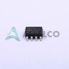
SOIC-8 package for space-saving design
Product Advantages
Excellent high-frequency performance
Precise signal conditioning and amplification
Low power consumption
Wide operating temperature range
Compact surface-mount package
Key Technical Parameters
Gain Bandwidth Product: 8 MHz
Supply Voltage Range: 10 V to 30 V
Input Offset Voltage: 80 μV
Input Bias Current: 25 pA
Output Current per Channel: 70 mA
Slew Rate: 20 V/μs
Operating Temperature Range: -40°C to 125°C
Quality and Safety Features
RoHS3 compliant
Reliable and durable construction
Thorough testing and quality control
Compatibility
Suitable for a wide range of instrumentation and control applications
Application Areas
Precision measurement and control systems
High-speed data acquisition
Analog signal conditioning
Professional audio and video equipment
Industrial automation and process control
Product Lifecycle
Currently in production
Mature product with long-term availability
Replacement parts and upgrades readily available
Several Key Reasons to Choose This Product
Excellent high-frequency performance for demanding applications
Low noise and input bias current for precise signal conditioning
Wide supply voltage range and high output current capability
Compact SOIC-8 package for space-saving design
Reliable and durable construction with RoHS3 compliance
Compatibility with a wide range of instrumentation and control applications
 AD8513ARUZAnalog Devices Inc.IC OPAMP JFET 4 CIRCUIT 14TSSOP
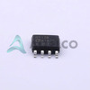 AD8512BRZAnalog Devices Inc.IC OPAMP JFET 2 CIRCUIT 8SOIC
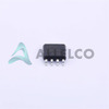 AD8512ARZ-REELAnalog Devices Inc.IC OPAMP JFET 2 CIRCUIT 8SOIC
 AD8513ARUZ-REELAnalog Devices Inc.IC OPAMP JFET 4 CIRCUIT 14TSSOP
 AD8513ARAnalog Devices Inc.IC OPAMP JFET 4 CIRCUIT 14SOIC
 AD8512BR


