View All

Please refer to the English Version as our Official Version.Return

Europe
France(Français) Germany(Deutsch) Italy(Italia) Russian(русский) Poland(polski) Czech(Čeština) Luxembourg(Lëtzebuergesch) Netherlands(Nederland) Iceland(íslenska) Hungarian(Magyarország) Spain(español) Portugal(Português) Turkey(Türk dili) Bulgaria(Български език) Ukraine(Україна) Greece(Ελλάδα) Israel(עִבְרִית) Sweden(Svenska) Finland(Svenska) Finland(Suomi) Romania(românesc) Moldova(românesc) Slovakia(Slovenská) Denmark(Dansk) Slovenia(Slovenija) Slovenia(Hrvatska) Croatia(Hrvatska) Serbia(Hrvatska) Montenegro(Hrvatska) Bosnia and Herzegovina(Hrvatska) Lithuania(lietuvių) Spain(Português) Switzerland(Deutsch) United Kingdom(English)
Asia/Pacific
Japan(日本語) Korea(한국의) Thailand(ภาษาไทย) Malaysia(Melayu) Singapore(Melayu) Vietnam(Tiếng Việt) Philippines(Pilipino)
Africa, India and Middle East
United Arab Emirates(العربية) Iran(فارسی) Tajikistan(فارسی) India(हिंदी) Madagascar(malaɡasʲ)
South America / Oceania
New Zealand(Maori) Brazil(Português) Angola(Português) Mozambique(Português)
North America
United States(English) Canada(English) Haiti(Ayiti) Mexico(español)
HomeProductsIntegrated Circuits (ICs)Linear - Amplifiers - Instrumentation, OP Amps, Buffer AmpsAD8513AR-REEL7
Image may be representation.
See specifications for product details.
EXPRESS OPTION
Payment method

AD8513AR-REEL7 - Analog Devices Inc.

Manufacturer Part Number
AD8513AR-REEL7
Manufacturer
Analog Devices, Inc.
Allelco Part Number
32D-AD8513AR-REEL7
Warranty
1 Year Allelco Warranty - Find out more
Stock Status:
4,890 pcs available, New & Original
Parts Description
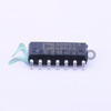
IC OPAMP JFET 4 CIRCUIT 14SOIC
Package
14-SOIC
Data sheet
AD8513AR-REEL7.pdf

Datasheets

AD8510,12,13.pdf

Other Related Documents

Tape and Reel Packaging.pdf
RoHs Status
 
Our certification
In stock: 4890

Required fields are indicated by an asterisk (*)
Please send RFQ, we will respond immediately.

Quantity

Specifications

AD8513AR-REEL7 Tech Specifications
Analog Devices Inc. - AD8513AR-REEL7 technical specifications, attributes, parameters and parts with similar specifications to Analog Devices Inc. - AD8513AR-REEL7

Product Attribute Attribute Value
Manufacturer Analog Devices, Inc.
Voltage - Supply Span (Min) 10 V
Voltage - Supply Span (Max) 30 V
Voltage - Input Offset 100 µV
Supplier Device Package 14-SOIC
Slew Rate 20V/µs
Series -
Package / Case 14-SOIC (0.154", 3.90mm Width)
Package Tape & Reel (TR)
Output Type -
Product Attribute Attribute Value
Operating Temperature -40°C ~ 125°C
Number of Circuits 4
Mounting Type Surface Mount
Gain Bandwidth Product 8 MHz
Current - Supply 2.2mA (x4 Channels)
Current - Output / Channel 70 mA
Current - Input Bias 25 pA
Base Product Number AD8513
Amplifier Type J-FET

Environmental & Export Classifications

ATTRIBUTE DESCRIPTION
Moisture Sensitivity Level (MSL) 1 (Unlimited)
ECCN EAR99

Frequently Asked Questions(FAQ)

How does the AD8513AR-REEL7 compare to other JFET-input operational amplifiers in terms of input bias current and noise performance for precision analog signal conditioning applications?
The AD8513AR-REEL7 features an exceptionally low input bias current of 25 pA, which is significantly lower than many competing JFET op-amps such as the TL084 series that typically exhibit bias currents in the nanoampere range. This characteristic makes it particularly suitable for high-impedance sensor interface circuits where leakage current can introduce significant offset errors. When combined with its low voltage input offset of 100 µV, the device provides superior DC accuracy compared to general-purpose JFET amplifiers. For precision applications requiring minimal charge injection and long-term stability, this combination of parameters enables accurate amplification of microvolt-level signals from thermocouples or piezoelectric sensors without introducing substantial drift over time.
What are the key limitations of the AD8513AR-REEL7 when used in high-gain feedback configurations above 60 dB, and how do these constraints impact circuit stability?
At closed-loop gains exceeding 60 dB, the AD8513AR-REEL7 exhibits reduced phase margin due to its internal compensation architecture and limited slew rate of 20 V/µs. The gain-bandwidth product of 8 MHz becomes a critical factor, as higher closed-loop gains reduce the effective bandwidth according to the relationship f = GBW / (1 + A_CL). For a 1000x (60 dB) gain configuration, the usable bandwidth drops to approximately 8 kHz, which may be insufficient for wideband signals. Additionally, the 20 V/µs slew rate imposes transient limitations—any output step larger than 20 × V_pp × f_max will cause distortion. These characteristics necessitate careful layout and component selection in precision instrumentation designs to avoid oscillation or settling issues.
Can the AD8513AR-REEL7 be safely operated in single-supply configurations below 10 V, and what modifications are required for proper functionality in low-voltage battery-powered systems?
The AD8513AR-REEL7 requires a minimum supply span of 10 V across both rails, meaning it cannot operate properly with a single supply below 10 V unless negative rail extension is implemented. For true single-supply operation down to 5 V, designers must use external level-shifting circuitry or choose a different amplifier family rated for rail-to-rail input/output and sub-5 V supplies. Attempting to operate the AD8513AR-REEL7 with a 5 V single supply without additional circuitry results in degraded common-mode rejection, increased offset voltage, and potential saturation of the input stage. Therefore, in low-power embedded systems where 5 V or lower operation is required, alternative solutions such as using a dedicated low-voltage JFET or CMOS op-amp should be considered instead of modifying the supply scheme around the AD8513AR-REEL7.
In what scenarios would the AD8513AR-REEL7 outperform CMOS-based quad op-amps like the ADA4610-4ARZ-RL despite having lower output drive capability?
The AD8513AR-REEL7 offers distinct advantages over CMOS alternatives such as the ADA4610-4ARZ-RL in applications involving high-impedance sources and long cable runs due to its ultra-low input bias current (25 pA vs. typical nA levels in CMOS devices). This makes it ideal for photodiode transimpedance amplifiers or electrochemical sensing interfaces where minimizing loading effects on the source is critical. While the ADA4610-4ARZ-RL delivers higher output current (up to 20 mA per channel), the AD8513AR-REEL7’s superior dc precision and lower flicker noise make it more suitable for static or slowly varying measurements. Furthermore, in environments with large electromagnetic interference, the JFET input stage of the AD8513AR-REEL7 provides better immunity to capacitive coupling-induced transients compared to the metal-oxide-semiconductor inputs of CMOS parts.
What thermal and power considerations should engineers evaluate when integrating the AD8513AR-REEL7 into a compact PCB design with multiple amplifier channels?
Each channel of the AD8513AR-REEL7 consumes approximately 2.2 mA at typical supply voltages, resulting in a total quiescent current of roughly 8.8 mA for all four channels. At a 12 V supply, this translates to about 105.6 mW of power dissipation per package. Engineers must account for this in thermal modeling, especially in space-constrained designs where heat sinking is limited. Although the 14-SOIC package has moderate thermal resistance, continuous operation near maximum temperature (125°C ambient) requires derating or airflow consideration. Additionally, the high supply voltage tolerance up to 30 V allows flexibility but increases risk of excessive power dissipation if output stages saturate frequently. Proper decoupling and layout practices help mitigate localized heating and ensure reliable operation across the full industrial temperature range.
How does the operating temperature range of the AD8513AR-REEL7 influence its suitability for automotive or industrial control systems, and what failure modes might emerge outside recommended conditions?
With an extended operating temperature range from -40°C to 125°C, the AD8513AR-REEL7 meets stringent requirements for automotive and industrial environments where thermal cycling and elevated temperatures are common. However, prolonged exposure beyond 125°C accelerates electromigration in the JFET gate oxide, leading to gradual degradation of input bias current and offset voltage over time. At cryogenic temperatures near -40°C, input capacitance increases slightly, affecting high-frequency response but not rendering the device nonfunctional. The absence of tin whisker concerns due to lead-free packaging further enhances reliability in harsh conditions. Nevertheless, users must validate long-term drift characteristics under actual system stress profiles, as datasheet specifications represent worst-case values under controlled laboratory conditions.
What layout and grounding strategies are essential to maintain the AD8513AR-REEL7’s low-noise performance in mixed-signal systems with digital switching components?
To preserve the low noise floor and high CMRR of the AD8513AR-REEL7, engineers should implement separate analog and digital ground planes connected through a single-point star connection near the power entry point. The 14-SOIC footprint demands careful attention to trace impedance matching and minimizing parasitic inductance in supply bypass networks—using 0.1 µF ceramic capacitors placed within 5 mm of each V+ pin reduces high-frequency impedance. Guard rings around sensitive nodes help shield against capacitive coupling from nearby digital aggressors. Additionally, routing input traces away from clock lines and switching regulators prevents substrate injection into the JFET input stage, which could elevate input offset voltage temporarily during transitions.
When substituting the AD8513AR-REEL7 with alternate parts like the TL084ACDT or ADA4610-4ARZ-RL, what critical parameter mismatches must be verified to prevent functional failure?
Substituting the AD8513AR-REEL7 requires careful evaluation of input bias current, supply voltage compatibility, and output swing limitations. While the TL084ACDT shares similar pinout and package, its input bias current (~30 pA typ) is comparable but offset voltage tends to be higher (~1 mV max), potentially degrading precision in gain stages below 10,000. The ADA4610-4ARZ-RL, though functionally similar, uses CMOS inputs with much higher input bias current (~1 pA typical but subject to variability), making it less predictable in high-resistance divider networks. Both substitutes have different slew rates and power consumption profiles; the TL084 series draws ~1.8 mA/channel versus the AD8513AR-REEL7’s 2.2 mA, while the ADA4610 consumes significantly less current (~1 mA total). Ensuring adequate headroom for output compliance and verifying unity-gain stability under expected load conditions prevents oscillation or distorted waveforms post-substitution.

Parts with Similar Specifications

The three parts on the right have similar specifications to Analog Devices Inc. AD8513AR-REEL7

Product Attribute AD8513ARZ-REEL7 AD8513ARUZ-REEL AD8513AR-REEL AD8513ARU-REEL
Part Number AD8513ARZ-REEL7 AD8513ARUZ-REEL AD8513AR-REEL AD8513ARU-REEL
Manufacturer Analog Devices Inc. Analog Devices Inc. Analog Devices Inc. Analog Devices Inc.
Package - Tape & Reel (TR) Tube Tape & Reel (TR)
Supplier Device Package - 196-NFBGA (12x12) 16-PDIP 64-VQFN (9x9)
Amplifier Type - - - -
Base Product Number - DAC34H84 MAX500 ADS62P42
Slew Rate - - - -
Package / Case - 196-LFBGA 16-DIP (0.300', 7.62mm) 64-VFQFN Exposed Pad
Mounting Type - Surface Mount Through Hole Surface Mount
Output Type - Current - Unbuffered Voltage - Buffered -
Voltage - Supply Span (Min) - - - -
Gain Bandwidth Product - - - -
Current - Supply - - - -
Current - Input Bias - - - -
Current - Output / Channel - - - -
Series - - - -
Voltage - Supply Span (Max) - - - -
Voltage - Input Offset - - - -
Number of Circuits - - - -
Operating Temperature - -40°C ~ 85°C 0°C ~ 70°C -40°C ~ 85°C

AD8513AR-REEL7 Datasheet PDF

Download AD8513AR-REEL7 pdf datasheets and Analog Devices Inc. documentation for AD8513AR-REEL7 - Analog Devices Inc..

Datasheets
AD8510,12,13.pdf
Other Related Documents
Tape and Reel Packaging.pdf
PCN Obsolescence/ EOL
EOL Lead (Pb)-Bearing 07/Oct/2016.pdf

Customer Reviews

Evaluation: 10 Articles

  • Nath***rooks
    Jun 11, 2026

    Installed this power component in a converter board. Output remained stable under different load conditions and thermal performance was better than expected.

  • Dani***alkerTech
    Jun 1, 2026

    Product works, but setup took more effort than expected. Once configured the MCU ran reliably, although documentation support felt older compared with newer platforms. Fine for maintenance projects.

  • Yuki***aka88
    May 26, 2026

    信号通信プロジェクトでこのRS-485トランシーバーを使用しました。設置は簡単で、長距離ケーブルでも通信は安定していました。消費電力も、以前使用していたものより低くなっています。

  • Stev***aker
    May 20, 2026

    Solid diode for power rectification. Works well in switching circuits.

  • Bran***Lewis
    May 11, 2026

    Compact FPGA with good performance. Suitable for basic signal processing tasks.

  • Oliv***arris
    May 7, 2026

    Reliable I/O expander. Works well in embedded control applications.

  • Jess***Jones
    Apr 17, 2026

    It offers good value for the price, and the specifications match the description. I’ve been using it for two days with no issues, and I’ll definitely buy it again if I need it in the future.

  • Mich***Smith
    Apr 17, 2026

    Shipping was on time, the component pins are neatly aligned, and I tested 10 of them with a multimeter—all readings were within the specified range. Highly recommended.

  • Aman***arris
    Apr 3, 2026

    It was great—the entire process, from placing the order to receiving the package, went very smoothly. The components were consistent, the price was fair, and I had a very pleasant shopping experience.

  • Mike***nch
    Apr 3, 2026

    Better than expected! The resistance and capacitance readings were spot-on, and it passed the test on the first try. The service was reliable, and the packaging was thoughtful—I highly recommend it.

Write a Review

Your Email address will not be published.

Shipment

Delivery Time

In-stock items can be shipped within 24 hours. Some parts will be arranged for delivery within 1-2 days from the date all items arrive at our warehouse. And Allelco ships order once a day at about 17:00, except Sunday. Once the goods are shipped, the estimated delivery time depends on the shipping methods and Delivery destination. The table below shows are the logistic time for some common countries.

Delivery Cost

  1. Use your express account for shipment if you have one.
  2. Use our account for the shipment. Refer to the table below for the approximate charges.
(Different time frame / countries / package size has different price.)

Delivery Method

  1. Global Common Shipment by DHL / UPS / FedEx / TNT / EMS / SF we support.
  2. Others more shipping ways, please get in touch with your customer manager.

Common Countries Logistic Time Reference
Region Country Logistic Time(Day)
America United States 5
Brazil 7
Europe Germany 5
United Kingdom 4
Italy 5
Oceania Australia 6
New Zealand 5
Asia India 4
Japan 4
Middle East Israel 6
DHL & FedEx Shipment Charges Reference
Shipment charges(KG) Reference DHL(USD$)
0.00kg-1.00kg USD$30.00 - USD$60.00
1.00kg-2.00kg USD$40.00 - USD$80.00
2.00kg-3.00kg USD$50.00 - USD$100.00
Note:
The above table is for reference only. There may have some data bias for the uncontrollable factors.
Contact us if you have any questions.
  • QC (Quality Warranty)
  • Payment Support
  • Packaging
  • Certifications & Memberships

QC (Quality Warranty)

Allelco is committed to exceeding customer expectations through customer service excellence, order accuracy, and on-time delivery.
This is achieved through our commitment to the continual improvement of our processes, services, and products.


Strict quality inspection builds a solid foundation for electronic component quality.
  1. Visual inspection
  2. Performance testing and reliability verification
  3. Standardized full-process testing
  4. Precise control of every parameter
We eliminate defective components and ensure the stable operation of electronic devices through professional quality standards.

Payment Support

The payment method can be chosen from the methods shown below: Wire Transfer (T/T, Bank Transfer), Western Union, Credit card, PayPal.
  • HKBea
  • Paypal
  • MasterCard
  • Western-Union
  • VISA
Stable Delivery, Sincere Partnership — Your Faithful Supply Chain Partner
  • Efficient Supply Management
  • Cost-Saving Procurement
  • Fast Sourcing & Delivery
Contact us if you have any questions.

Packaging

Electrostatic Discharge Protection and Handling

All electrostatic-sensitive components are handled in accordance with electrostatic discharge control procedures. The products are hermetically sealed in anti-static safe packaging to prevent electrostatic damage. Appropriate labeling is also applied for identification and traceability. This ensures product integrity during storage, handling and transportation.


ESD

Certifications & Memberships

Third-party certified, strict quality control. Our certification
  • ISO 9001: 2015
  • ISO 13485: 2016
  • ISO 14001: 2015
  • ISO 28000: 2007
  • ISO 45001: 2018
  • GB/T 27922-2011
  • SMTA
  • IPC
  • ESD
  • PSMA
Analog Devices Inc.

AD8513AR-REEL7

Analog Devices Inc.
32D-AD8513AR-REEL7

Want a better price? Add to Cart and Submit RFQ now, we'll contact you immediately.

0 RFQ
Shopping cart (0 Items)
It is empty.
Compare List (0 Items)
It is empty.
Feedback

Your feedback matters! At Allelco, we value the user experience and strive to improve it constantly.
Please share your comments with us via our feedback form, and we'll respond promptly.
Thank you for choosing Allelco.

Subject
E-mail
Comments
Captcha
Drag or click to upload file
Upload File
types: .xls, .xlsx, .doc, .docx, .jpg, .png and .pdf.
Max file size: 10MB