
AD8513ARUZ (1)
Manufacturer Part Number
AD8513ARUZ
Manufacturer
Analog Devices, Inc.
Introduction
Precision, quad, JFET-input operational amplifier
Product Features and Performance
4 independent op-amp channels
High input impedance
Low input bias current
Low input offset voltage
Wide supply voltage range
High output current capability
Wide bandwidth of 8 MHz
High slew rate of 20 V/μs
Excellent DC and AC performance
Product Advantages
Precise and stable performance
Low noise operation
Reliable and robust design
Suitable for a wide range of applications
Key Technical Parameters
Supply voltage range: 10 V to 30 V
Input offset voltage: 100 μV
Input bias current: 25 pA
Gain bandwidth product: 8 MHz
Slew rate: 20 V/μs
Output current per channel: 70 mA
Quality and Safety Features
RoHS3 compliant
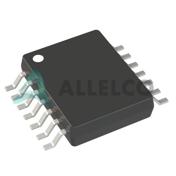
14-TSSOP package
Compatibility
Surface mount design
Suitable for a wide range of applications
Application Areas
Instrumentation and measurement
Data acquisition systems
Medical equipment
Industrial control systems
Product Lifecycle
The AD8513ARUZ is an active product, and Analog Devices continues to support it. Replacement or upgraded options may be available in the future.
Key Reasons to Choose This Product
Excellent precision and stability
Wide operating voltage and temperature range
High output current capability
Reliable and robust performance
Suitable for a variety of applications

 AD8512BRZ-REEL7Analog Devices Inc.IC OPAMP JFET 2 CIRCUIT 8SOIC
 AD8515AKS-R2Analog Devices Inc.IC AMP GP R-R CMOS 5MHZ SC70-5
 AD8513ARZ-REEL7Analog Devices Inc.IC OPAMP JFET 4 CIRCUIT 14SOIC


