View All

Please refer to the English Version as our Official Version.Return

Europe
France(Français) Germany(Deutsch) Italy(Italia) Russian(русский) Poland(polski) Czech(Čeština) Luxembourg(Lëtzebuergesch) Netherlands(Nederland) Iceland(íslenska) Hungarian(Magyarország) Spain(español) Portugal(Português) Turkey(Türk dili) Bulgaria(Български език) Ukraine(Україна) Greece(Ελλάδα) Israel(עִבְרִית) Sweden(Svenska) Finland(Svenska) Finland(Suomi) Romania(românesc) Moldova(românesc) Slovakia(Slovenská) Denmark(Dansk) Slovenia(Slovenija) Slovenia(Hrvatska) Croatia(Hrvatska) Serbia(Hrvatska) Montenegro(Hrvatska) Bosnia and Herzegovina(Hrvatska) Lithuania(lietuvių) Spain(Português) Switzerland(Deutsch) United Kingdom(English)
Asia/Pacific
Japan(日本語) Korea(한국의) Thailand(ภาษาไทย) Malaysia(Melayu) Singapore(Melayu) Vietnam(Tiếng Việt) Philippines(Pilipino)
Africa, India and Middle East
United Arab Emirates(العربية) Iran(فارسی) Tajikistan(فارسی) India(हिंदी) Madagascar(malaɡasʲ)
South America / Oceania
New Zealand(Maori) Brazil(Português) Angola(Português) Mozambique(Português)
North America
United States(English) Canada(English) Haiti(Ayiti) Mexico(español)
HomeProductsIntegrated Circuits (ICs)Linear - Amplifiers - Instrumentation, OP Amps, Buffer AmpsAD8513AR
Image may be representation.
See specifications for product details.
EXPRESS OPTION
Payment method

AD8513AR - Analog Devices Inc.

Manufacturer Part Number
AD8513AR
Manufacturer
Analog Devices, Inc.
Allelco Part Number
32D-AD8513AR
Warranty
1 Year Allelco Warranty - Find out more
Stock Status:
16,730 pcs available, New & Original
Parts Description
IC OPAMP JFET 4 CIRCUIT 14SOIC
Package
14-SOIC
Data sheet
AD8513AR.pdf

Datasheets

AD8510,12,13.pdf
RoHs Status
 
Our certification
In stock: 16730

Required fields are indicated by an asterisk (*)
Please send RFQ, we will respond immediately.

Quantity

Specifications

AD8513AR Tech Specifications
Analog Devices Inc. - AD8513AR technical specifications, attributes, parameters and parts with similar specifications to Analog Devices Inc. - AD8513AR

Product Attribute Attribute Value
Manufacturer Analog Devices, Inc.
Voltage - Supply Span (Min) 10 V
Voltage - Supply Span (Max) 30 V
Voltage - Input Offset 100 µV
Supplier Device Package 14-SOIC
Slew Rate 20V/µs
Series -
Package / Case 14-SOIC (0.154", 3.90mm Width)
Package Tube
Output Type -
Product Attribute Attribute Value
Operating Temperature -40°C ~ 125°C
Number of Circuits 4
Mounting Type Surface Mount
Gain Bandwidth Product 8 MHz
Current - Supply 2.2mA (x4 Channels)
Current - Output / Channel 70 mA
Current - Input Bias 25 pA
Base Product Number AD8513
Amplifier Type J-FET

Environmental & Export Classifications

ATTRIBUTE DESCRIPTION
Moisture Sensitivity Level (MSL) 1 (Unlimited)
ECCN EAR99

Parts Introduction

Manufacturer Part Number

AD8513AR

Manufacturer

Analog Devices, Inc.

Introduction

High-performance quad J-FET input operational amplifier

Suitable for instrumentation, buffer, and general-purpose amplifier applications

Product Features and Performance

Quad operational amplifier with 4 independent channels

High input impedance J-FET input stage

Very low input bias current of 25 pA

Wide supply voltage range of 10 V to 30 V

High gain-bandwidth product of 8 MHz

20 V/μs slew rate

Low input offset voltage of 100 μV

Able to drive capacitive loads up to 500 pF

Operating temperature range of -40°C to +125°C

Product Advantages

Excellent precision and stability for sensitive measurement applications

Wide operating voltage range allows use in a variety of systems

Low power consumption of 2.2 mA per channel

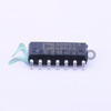
Compact 14-SOIC package saves board space

Key Technical Parameters

Manufacturer Part Number: AD8513AR

Number of Circuits: 4

Gain Bandwidth Product: 8 MHz

Voltage Supply Span (Min): 10 V

Current Supply: 2.2 mA (x4 Channels)

Slew Rate: 20 V/μs

Voltage Input Offset: 100 μV

Amplifier Type: J-FET

Voltage Supply Span (Max): 30 V

Current Output / Channel: 70 mA

Current Input Bias: 25 pA

Quality and Safety Features

Manufactured by Analog Devices, a leading provider of high-performance analog ICs

Specified for operation over the industrial temperature range of -40°C to +125°C

Robust 14-SOIC package suitable for surface mount assembly

Compatibility

Compatible with a wide range of electronic systems and circuits requiring high-performance, low-noise operational amplifiers

Application Areas

Instrumentation and measurement equipment

Buffer amplifiers

General-purpose amplifier circuits

Product Lifecycle

This product is currently in production and widely available

Analog Devices has a history of long-term support for their products, with availability of replacements and upgrades as needed

Several Key Reasons to Choose This Product

Excellent precision and stability for sensitive applications

Wide operating voltage range and low power consumption

Compact, space-saving 14-SOIC package

Proven reliability and long-term availability from a leading manufacturer

Frequently Asked Questions(FAQ)

What are the key performance trade-offs when selecting the AD8513AR for high-impedance sensor signal conditioning applications, and how does its input bias current compare to CMOS op-amps in similar gain bandwidth ranges?
The AD8513AR offers extremely low input bias current at 25 pA, which is significantly lower than typical CMOS op-amps such as the TL084 series, making it highly suitable for high-impedance sensor interfaces where leakage currents can distort small-signal measurements. However, this JFET-input characteristic comes with a higher voltage input offset of 100 µV compared to precision CMOS types like the OP07 or LT1007. While the AD8513AR provides a gain bandwidth product of 8 MHz and a slew rate of 20 V/µs—adequate for many analog front-end tasks—engineers must consider that its supply current per channel (2.2 mA) is higher than ultra-low-power CMOS alternatives. This trade-off favors signal integrity over power efficiency in battery-powered systems. For applications requiring sub-pA bias current and moderate bandwidth, the AD8513AR outperforms standard CMOS devices but may be overkill for digital signal processing stages where speed dominates.
How does the AD8513AR’s operating voltage range affect system design in industrial environments, and what considerations apply when interfacing with 5V logic or legacy control systems?
The AD8513AR supports a supply span from 10 V to 30 V, which limits its direct use in 5V digital systems without level-shifting circuitry or separate analog supplies. This makes integration into modern mixed-signal designs challenging unless careful partitioning between analog and digital domains is implemented. In industrial settings where 24V DC power rails are common, the device operates reliably within specification, offering robust noise immunity and stable output drive up to 70 mA per channel. Engineers should ensure proper decoupling and layout practices to maintain performance across the full temperature range (-40°C to 125°C). Using the AD8513AR in conjunction with lower-voltage microcontrollers requires attention to common-mode input range compatibility and output swing headroom relative to ground.
When comparing the AD8513AR to the TL084CDT for audio preamplifier applications, which device offers better noise performance and why?
The AD8513AR generally delivers superior noise performance due to its lower input-referred voltage noise density and exceptionally low input bias current, which reduces thermal noise contributions from source resistances. While both devices share similar gain bandwidth products (~8 MHz), the AD8513AR’s JFET inputs exhibit lower flicker (1/f) noise at low frequencies compared to the bipolar input stage of the TL084CDT. Additionally, the AD8513AR’s higher slew rate (20 V/µs vs. typically ~13 V/µs for TL084) enables cleaner handling of transient signals in audio paths. However, the TL084CDT benefits from wider availability and broader historical support in legacy audio designs. For high-impedance microphone or piezoelectric sensor conditioning, the AD8513AR minimizes loading effects and preserves signal fidelity better than the TL084CDT.
What layout and thermal management strategies are recommended when using multiple AD8513AR channels in close proximity on a compact PCB?
Each channel in the AD8513AR draws approximately 2.2 mA under normal conditions, so four channels consume around 8.8 mA total—a relatively modest load. Nevertheless, thermal coupling between adjacent channels can affect long-term drift and offset stability, especially at elevated ambient temperatures near 125°C. A recommended practice is to maintain minimum spacing of 1.5 mm between SOIC pads and allocate adequate copper pour beneath the package for heat spreading. Ground plane continuity under the IC enhances stability and reduces susceptibility to electromagnetic interference. Avoid routing high-speed digital traces parallel to analog signal paths above the amplifier layer to prevent capacitive crosstalk. Proper decoupling with 100 nF ceramic capacitors placed within 5 mm of each V+ pin further ensures clean power delivery across the 10–30 V range.
Can the AD8513AR be used in single-supply configurations below 10 V, and what compromises arise if forced into such operation?
Operating the AD8513AR below 10 V violates its specified supply voltage minimum and risks degraded performance or undefined behavior. Attempting to run it at 5 V would severely limit the available output swing and reduce headroom for input common-mode range, potentially driving the inputs outside the linear region. Furthermore, internal biasing circuits rely on sufficient supply voltage to maintain proper transistor operation, and sub-10 V operation could increase offset voltage drift and bias current variability. While some op-amps tolerate brief undervoltage conditions gracefully, continuous operation below 10 V on the AD8513AR is not supported and may lead to erratic outputs or damage over time. For low-voltage applications, alternative parts like the LMV324 or MCP604 are more appropriate.
How does the moisture sensitivity level (MSL) rating of MSL 1 for the AD8513AR impact handling and storage in high-humidity manufacturing environments?
With an MSL rating of 1, the AD8513AR has unlimited shelf life and does not require special drying procedures prior to reflow soldering, even after prolonged exposure to ambient humidity. This simplifies inventory management and reduces handling protocols in high-humidity facilities. Standard JEDEC-compliant dry packaging ensures reliability during wave or reflow soldering without risk of popcorning or delamination. As long as ESD precautions are observed during unpacking and assembly, the device maintains consistent solder joint quality and long-term performance. This classification reflects Analog Devices’ confidence in the package’s robustness and aligns with industry standards for lead-free, surface-mount components like the 14-SOIC variant.
In what scenarios would substituting the AD8513AR with the TL3474ACD improve overall system reliability, despite differences in architecture?
The TL3474ACD, a CMOS-input quad op-amp, may offer improved immunity to electrostatic discharge (ESD) and reduced susceptibility to latch-up compared to the AD8513AR’s JFET inputs, making it preferable in harsh industrial environments with frequent hot-plugging or inductive load switching. While the TL3474ACD typically exhibits higher input bias current (nA range vs. 25 pA), it consumes less power per channel and operates reliably down to 3 V, enabling lower-voltage designs. If system-level ESD protection is insufficient and the application involves frequent mechanical connections, the TL3474ACD’s enhanced ruggedness could outweigh the AD8513AR’s superior DC precision. However, for instrumentation with high source impedance (>1 MΩ), the AD8513AR remains the better choice due to minimal leakage.
What role does the gain bandwidth product (GBW = 8 MHz) play in determining maximum usable closed-loop gain for the AD8513AR in feedback configurations?
The 8 MHz gain bandwidth product defines the frequency at which open-loop gain drops by 3 dB relative to DC values. In closed-loop configurations, the usable bandwidth decreases as gain increases, following the relationship f_unity_gain = GBW / A_CL. For example, a gain of 100 yields a bandwidth of approximately 80 kHz, while a gain of 10 reduces it to 800 kHz. This trade-off constrains high-gain, wideband applications such as active filters or transimpedance amplifiers. Engineers must verify that the desired signal bandwidth fits within the available gain-bandwidth budget. At unity gain, the AD8513AR can deliver full-speed response, making it suitable for buffer or comparator-like roles where stability and slew rate dominate over voltage amplification.

Parts with Similar Specifications

The three parts on the right have similar specifications to Analog Devices Inc. AD8513AR

Product Attribute AD8513ARZ-REEL AD8513ARZ-REEL7 AD8513ARUZ AD8513AR-REEL
Part Number AD8513ARZ-REEL AD8513ARZ-REEL7 AD8513ARUZ AD8513AR-REEL
Manufacturer Analog Devices Inc. Analog Devices Inc. Analog Devices Inc. Analog Devices Inc.
Output Type - Current - Unbuffered Voltage - Buffered -
Base Product Number - DAC34H84 MAX500 ADS62P42
Package / Case - 196-LFBGA 16-DIP (0.300', 7.62mm) 64-VFQFN Exposed Pad
Current - Output / Channel - - - -
Amplifier Type - - - -
Mounting Type - Surface Mount Through Hole Surface Mount
Series - - - -
Voltage - Supply Span (Min) - - - -
Operating Temperature - -40°C ~ 85°C 0°C ~ 70°C -40°C ~ 85°C
Slew Rate - - - -
Voltage - Input Offset - - - -
Number of Circuits - - - -
Voltage - Supply Span (Max) - - - -
Supplier Device Package - 196-NFBGA (12x12) 16-PDIP 64-VQFN (9x9)
Current - Supply - - - -
Current - Input Bias - - - -
Package - Tape & Reel (TR) Tube Tape & Reel (TR)
Gain Bandwidth Product - - - -

AD8513AR Datasheet PDF

Download AD8513AR pdf datasheets and Analog Devices Inc. documentation for AD8513AR - Analog Devices Inc..

Datasheets
AD8510,12,13.pdf
PCN Obsolescence/ EOL
EOL Lead (Pb)-Bearing 07/Oct/2016.pdf

Customer Reviews

Evaluation: 10 Articles

  • Nath***rooks
    Jun 11, 2026

    Installed this power component in a converter board. Output remained stable under different load conditions and thermal performance was better than expected.

  • Dani***alkerTech
    Jun 1, 2026

    Product works, but setup took more effort than expected. Once configured the MCU ran reliably, although documentation support felt older compared with newer platforms. Fine for maintenance projects.

  • Yuki***aka88
    May 26, 2026

    信号通信プロジェクトでこのRS-485トランシーバーを使用しました。設置は簡単で、長距離ケーブルでも通信は安定していました。消費電力も、以前使用していたものより低くなっています。

  • Stev***aker
    May 20, 2026

    Solid diode for power rectification. Works well in switching circuits.

  • Bran***Lewis
    May 11, 2026

    Compact FPGA with good performance. Suitable for basic signal processing tasks.

  • Oliv***arris
    May 7, 2026

    Reliable I/O expander. Works well in embedded control applications.

  • Jess***Jones
    Apr 17, 2026

    It offers good value for the price, and the specifications match the description. I’ve been using it for two days with no issues, and I’ll definitely buy it again if I need it in the future.

  • Mich***Smith
    Apr 17, 2026

    Shipping was on time, the component pins are neatly aligned, and I tested 10 of them with a multimeter—all readings were within the specified range. Highly recommended.

  • Aman***arris
    Apr 3, 2026

    It was great—the entire process, from placing the order to receiving the package, went very smoothly. The components were consistent, the price was fair, and I had a very pleasant shopping experience.

  • Mike***nch
    Apr 3, 2026

    Better than expected! The resistance and capacitance readings were spot-on, and it passed the test on the first try. The service was reliable, and the packaging was thoughtful—I highly recommend it.

Write a Review

Your Email address will not be published.

Shipment

Delivery Time

In-stock items can be shipped within 24 hours. Some parts will be arranged for delivery within 1-2 days from the date all items arrive at our warehouse. And Allelco ships order once a day at about 17:00, except Sunday. Once the goods are shipped, the estimated delivery time depends on the shipping methods and Delivery destination. The table below shows are the logistic time for some common countries.

Delivery Cost

  1. Use your express account for shipment if you have one.
  2. Use our account for the shipment. Refer to the table below for the approximate charges.
(Different time frame / countries / package size has different price.)

Delivery Method

  1. Global Common Shipment by DHL / UPS / FedEx / TNT / EMS / SF we support.
  2. Others more shipping ways, please get in touch with your customer manager.

Common Countries Logistic Time Reference
Region Country Logistic Time(Day)
America United States 5
Brazil 7
Europe Germany 5
United Kingdom 4
Italy 5
Oceania Australia 6
New Zealand 5
Asia India 4
Japan 4
Middle East Israel 6
DHL & FedEx Shipment Charges Reference
Shipment charges(KG) Reference DHL(USD$)
0.00kg-1.00kg USD$30.00 - USD$60.00
1.00kg-2.00kg USD$40.00 - USD$80.00
2.00kg-3.00kg USD$50.00 - USD$100.00
Note:
The above table is for reference only. There may have some data bias for the uncontrollable factors.
Contact us if you have any questions.
  • QC (Quality Warranty)
  • Payment Support
  • Packaging
  • Certifications & Memberships

QC (Quality Warranty)

Allelco is committed to exceeding customer expectations through customer service excellence, order accuracy, and on-time delivery.
This is achieved through our commitment to the continual improvement of our processes, services, and products.


Strict quality inspection builds a solid foundation for electronic component quality.
  1. Visual inspection
  2. Performance testing and reliability verification
  3. Standardized full-process testing
  4. Precise control of every parameter
We eliminate defective components and ensure the stable operation of electronic devices through professional quality standards.

Payment Support

The payment method can be chosen from the methods shown below: Wire Transfer (T/T, Bank Transfer), Western Union, Credit card, PayPal.
  • HKBea
  • Paypal
  • MasterCard
  • Western-Union
  • VISA
Stable Delivery, Sincere Partnership — Your Faithful Supply Chain Partner
  • Efficient Supply Management
  • Cost-Saving Procurement
  • Fast Sourcing & Delivery
Contact us if you have any questions.

Packaging

Electrostatic Discharge Protection and Handling

All electrostatic-sensitive components are handled in accordance with electrostatic discharge control procedures. The products are hermetically sealed in anti-static safe packaging to prevent electrostatic damage. Appropriate labeling is also applied for identification and traceability. This ensures product integrity during storage, handling and transportation.


ESD

Certifications & Memberships

Third-party certified, strict quality control. Our certification
  • ISO 9001: 2015
  • ISO 13485: 2016
  • ISO 14001: 2015
  • ISO 28000: 2007
  • ISO 45001: 2018
  • GB/T 27922-2011
  • SMTA
  • IPC
  • ESD
  • PSMA
Analog Devices Inc.

AD8513AR

Analog Devices Inc.
32D-AD8513AR

Want a better price? Add to Cart and Submit RFQ now, we'll contact you immediately.

0 RFQ
Shopping cart (0 Items)
It is empty.
Compare List (0 Items)
It is empty.
Feedback

Your feedback matters! At Allelco, we value the user experience and strive to improve it constantly.
Please share your comments with us via our feedback form, and we'll respond promptly.
Thank you for choosing Allelco.

Subject
E-mail
Comments
Captcha
Drag or click to upload file
Upload File
types: .xls, .xlsx, .doc, .docx, .jpg, .png and .pdf.
Max file size: 10MB