 AD8512BRZ-REEL7Analog Devices Inc.IC OPAMP JFET 2 CIRCUIT 8SOIC
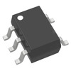 AD8515AKS-R2Analog Devices Inc.IC AMP GP R-R CMOS 5MHZ SC70-5
 AD8513ARU-REELAnalog Devices Inc.IC OPAMP JFET 8MHZ QUAD 14TSSOP
 AD8513ARUZ-REELAnalog Devices Inc.IC OPAMP JFET 4 CIRCUIT 14TSSOP
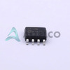 AD8512BRZAnalog Devices Inc.IC OPAMP JFET 2 CIRCUIT 8SOIC
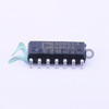 AD8513ARZ-REEL7Analog Devices Inc.IC OPAMP JFET 4 CIRCUIT 14SOIC
 AD8513ARZAnalog Devices Inc.IC OPAMP JFET 4 CIRCUIT 14SOIC
- Nath***rooks
- Jun 11, 2026

Image may be representation.
See specifications for product details.
See specifications for product details.
- EXPRESS OPTION
- Payment method
AD8513ARU - Analog Devices
- Manufacturer Part Number
- AD8513ARU
- Manufacturer
- Analog Devices, Inc.
- Allelco Part Number
- 41D-AD8513ARU
- Warranty
- 1 Year Allelco Warranty - Find out more
- Stock Status:
- 10,300 pcs available, New & Original
- Parts Description
- -
- Data sheet
- -
- Category
- Integrated Circuits (ICs) > Specialized ICs
- RoHs Status
- Our certification
- In stock: 10300
- Unit Price: $4.54
- Subtotal: $0.00
Want a better price?
Add to Cart and Submit RFQ now, we'll contact you immediately.
| Quantity | Unit Price | Ext. Price |
|---|---|---|
| 1+ | $4.54 | $4.54 |
| 200+ | $1.757 | $351.40 |
| 500+ | $1.695 | $847.50 |
| 1000+ | $1.665 | $1,665.00 |
The above prices does not include taxes and freight rates, which will be calculated on the order pages.


