View All

Please refer to the English Version as our Official Version.Return

Europe
France(Français) Germany(Deutsch) Italy(Italia) Russian(русский) Poland(polski) Czech(Čeština) Luxembourg(Lëtzebuergesch) Netherlands(Nederland) Iceland(íslenska) Hungarian(Magyarország) Spain(español) Portugal(Português) Turkey(Türk dili) Bulgaria(Български език) Ukraine(Україна) Greece(Ελλάδα) Israel(עִבְרִית) Sweden(Svenska) Finland(Svenska) Finland(Suomi) Romania(românesc) Moldova(românesc) Slovakia(Slovenská) Denmark(Dansk) Slovenia(Slovenija) Slovenia(Hrvatska) Croatia(Hrvatska) Serbia(Hrvatska) Montenegro(Hrvatska) Bosnia and Herzegovina(Hrvatska) Lithuania(lietuvių) Spain(Português) Switzerland(Deutsch) United Kingdom(English)
Asia/Pacific
Japan(日本語) Korea(한국의) Thailand(ภาษาไทย) Malaysia(Melayu) Singapore(Melayu) Vietnam(Tiếng Việt) Philippines(Pilipino)
Africa, India and Middle East
United Arab Emirates(العربية) Iran(فارسی) Tajikistan(فارسی) India(हिंदी) Madagascar(malaɡasʲ)
South America / Oceania
New Zealand(Maori) Brazil(Português) Angola(Português) Mozambique(Português)
North America
United States(English) Canada(English) Haiti(Ayiti) Mexico(español)
HomeProductsIntegrated Circuits (ICs)Embedded - MicroprocessorsOMAPL138BZCEA3
OMAPL138BZCEA3 Image
Image may be representation.
See specifications for product details.
EXPRESS OPTION
Payment method

OMAPL138BZCEA3 - Texas Instruments

Manufacturer Part Number
OMAPL138BZCEA3
Manufacturer
Texas Instruments
Allelco Part Number
32D-OMAPL138BZCEA3
Warranty
1 Year Allelco Warranty - Find out more
Stock Status:
9,030 pcs available, New & Original
Parts Description
IC MPU OMAP-L1X 375MHZ 361NFBGA
Package
361-NFBGA (13x13)
Data sheet
OMAPL138BZCEA3.pdf
RoHs Status
ROHS3 Compliant
Our certification
In stock: 9030

Required fields are indicated by an asterisk (*)
Please send RFQ, we will respond immediately.

Quantity

Specifications

OMAPL138BZCEA3 Tech Specifications
Texas Instruments - OMAPL138BZCEA3 technical specifications, attributes, parameters and parts with similar specifications to Texas Instruments - OMAPL138BZCEA3

Product Attribute Attribute Value
Manufacturer Texas Instruments
Voltage - I/O 1.8V, 3.3V
USB USB 1.1 + PHY (1), USB 2.0 + PHY (1)
Supplier Device Package 361-NFBGA (13x13)
Speed 375MHz
Series OMAP-L1x
Security Features Boot Security, Cryptography
SATA SATA 3Gbps (1)
RAM Controllers SDRAM
Package / Case 361-LFBGA
Package Tray
Product Attribute Attribute Value
Operating Temperature -40°C ~ 105°C (TJ)
Number of Cores/Bus Width 1 Core, 32-Bit
Mounting Type Surface Mount
Graphics Acceleration No
Ethernet 10/100Mbps (1)
Display & Interface Controllers LCD
Core Processor ARM926EJ-S
Co-Processors/DSP Signal Processing; C674x, System Control; CP15
Base Product Number OMAPL138
Additional Interfaces HPI, I²C, McASP, McBSP, MMC/SD, SPI, UART

Environmental & Export Classifications

ATTRIBUTE DESCRIPTION
RoHs Status ROHS3 Compliant
Moisture Sensitivity Level (MSL) 3 (168 Hours)
REACH Status REACH Unaffected
ECCN 3A991A2
HTSUS 8542.31.0001

Parts Introduction

OMAPL138BZCEA3 Image
OMAPL138BZCEA3 (1)

Manufacturer Part Number

OMAPL138BZCEA3

Manufacturer

Texas Instruments

Introduction

The OMAP-L138 processor is a low-power applications processor based on an ARM926EJ-S and a C674x DSP core.

Product Features and Performance

ARM926EJ-S Core

32-Bit Bus Width

DSP/Signal Processing with C674x

System Control with CP15

375MHz Operating Speed

SDRAM Memory Interface

LCD Display & Interface Controller

10/100Mbps Ethernet

SATA 3Gbps Interface

USB Interfaces with PHYs

No Graphics Acceleration

Product Advantages

Integrated ARM and DSP for versatile processing

High-speed interfaces for connectivity

Extended temperature range suitable for industrial applications

Boot Security and Cryptography features for secure operation

Key Technical Parameters

Core Processor: ARM926EJ-S

Number of Cores/Bus Width: 1 Core, 32-Bit

Speed: 375MHz

RAM Controllers: SDRAM

Ethernet: 10/100Mbps

SATA: SATA 3Gbps

USB: USB 1.1 and USB 2.0

Voltage I/O: 1.8V, 3.3V

Operating Temperature: -40°C to 105°C

Quality and Safety Features

Industrial temperature range for high reliability

Boot Security and Cryptography components for data protection

Compatibility

Various interfaces including HPI, I2C, McASP, McBSP, MMC/SD, SPI, UART

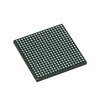
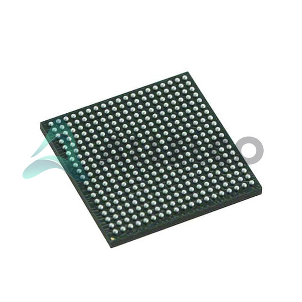
361-LFBGA Surface Mount Package

Application Areas

Industrial Control

Communication Infrastructure

Medical devices

Automotive

Product Lifecycle

Status: Obsolete

Information on replacements or upgrades may be available through Texas Instruments.

Several Key Reasons to Choose This Product

Combination of ARM and DSP cores for balanced processing power.

Robust connectivity options including Ethernet, SATA, and USB.

Advanced security via integrated features supporting secure boot and data encryption.

Suitable for harsh environments with wide operating temperature range.

Strong support and documentation from Texas Instruments, despite obsolescence.

Frequently Asked Questions(FAQ)

How does the OMAPL138BZCEA3 compare to other ARM9-based processors in terms of DSP integration and real-time signal processing performance, particularly when evaluating trade-offs between core frequency and co-processor capabilities?
The OMAPL138BZCEA3 integrates a C674x fixed-point DSP alongside the ARM926EJ-S core, enabling heterogeneous computing for real-time signal processing tasks. With a 375MHz ARM core and dedicated DSP at similar clock rates, it supports parallel execution of control logic and high-throughput algorithms such as audio coding or sensor fusion. Compared to single-core ARM9 devices without integrated DSPs, this architecture reduces latency and offloads computationally intensive operations from the main CPU. However, compared to higher-frequency Cortex-A series parts, the OMAP-L1x family trades peak instruction throughput for power efficiency and deterministic response—making it suitable for embedded systems requiring both Linux-capable processing and real-time peripheral handling.
What are the key considerations when selecting the OMAPL138BZCEA3 for an industrial application requiring secure boot and cryptographic acceleration, especially regarding hardware security features and their impact on system design complexity?
The OMAPL138BZCEA3 includes hardware-based boot security and cryptography support, which simplifies implementation of trusted boot chains and data encryption compared to software-only solutions. These features reduce reliance on external security chips but require careful configuration of the CP15 coprocessor and memory protection units. Engineers must account for the added firmware overhead during initialization and ensure that secure key storage aligns with physical access constraints. While this enhances tamper resistance, it also introduces dependencies on proper boot ROM code validation and secure partition management in the operating system layer.
In what scenarios would the dual USB interfaces (USB 1.1 + PHY and USB 2.0 + PHY) on the OMAPL138BZCEA3 be beneficial, and how should designers manage potential bandwidth conflicts or electrical isolation requirements?
The presence of both USB 1.1 and USB 2.0 ports allows flexible connectivity—for example, using USB 2.0 for high-speed host functions like mass storage while reserving USB 1.1 for low-bandwidth peripherals such as sensors or debug tools. This separation avoids contention on shared internal buses and improves system responsiveness. However, simultaneous full-speed transfers may stress the USB controller’s arbitration logic, necessitating careful endpoint allocation in firmware. Additionally, if isolation is required (e.g., medical or automotive environments), external galvanic barriers must be placed at the PHY level since the IC itself does not provide built-in isolation.
How does the OMAPL138BZCEA3 support display applications despite lacking dedicated graphics acceleration, and what limitations arise when driving high-resolution LCD panels compared to GPU-equipped SoCs?
Although the OMAPL138BZCEA3 lacks a dedicated GPU, it incorporates an LCD controller capable of driving standard resolutions up to WXGA (1280×768) at moderate frame rates through software-based pixel rendering or DMA-assisted transfers. This approach relies heavily on the ARM926EJ-S core and available RAM bandwidth—typically limiting sustained refresh rates above 30 fps for complex UIs. Compared to modern SoCs with hardware-accelerated 2D/3D engines, this imposes greater CPU load and restricts animation smoothness. Designers targeting richer visual interfaces often pair this MCU with an external display driver IC to offload timing-critical operations.
When comparing the OMAPL138BZCEA3 to newer-generation TI Sitara processors, what architectural advantages does its legacy ARM926EJ-S core offer in deterministic real-time control loops?
The ARM926EJ-S core in the OMAPL138BZCEA3 provides predictable interrupt latencies and simpler pipeline behavior compared to out-of-order superscalar cores found in Sitara AM3x or AM5x families. This makes it preferable for hard real-time subsystems where jitter minimization outweighs raw computational throughput. Its Tightly-Coupled Memory (TCM) interface allows deterministic access to instruction and data caches, which is critical in safety-certified applications like motor drives or industrial automation. While newer cores offer higher MFLOPS and multicore scalability, they introduce variable-latency memory hierarchies that complicate timing analysis.
What are the implications of the OMAPL138BZCEA3’s 1.8V/3.3V I/O voltage domains on mixed-signal PCB layout practices, especially when interfacing with legacy 5V TTL peripherals?
The OMAPL138BZCEA3 supports both 1.8V and 3.3V I/O rails, allowing partial voltage translation to accommodate older 5V logic families via level shifters. However, direct connection to 5V signals without buffering risks damaging the 1.8V-sensitive pins. Layout engineers should isolate noisy digital return currents from analog supplies, use guard rings around sensitive inputs, and place decoupling capacitors within 2 mm of power pins to maintain signal integrity across the mixed-voltage domain. Careful attention to ESD protection diodes and slew rate control further mitigates crosstalk in densely populated designs.
How does the SATA 3Gbps interface on the OMAPL138BZCEA3 affect system-level power consumption and thermal management in compact form factors?
Enabling the SATA port increases dynamic power draw due to PHY activation and link training sequences, contributing approximately 15–25 mA at 3.3V depending on activity. In thermally constrained enclosures, this necessitates adequate copper pour area under the BGA package and possibly airflow optimization to prevent junction temperatures exceeding 105°C. While SATA enables direct SSD connectivity without host bridge overhead, the associated heat generation can limit deployment in fanless or sealed industrial boxes unless power gating is implemented in firmware.
What role does the HPI interface play in the OMAPL138BZCEA3’s ecosystem, and how does it facilitate communication with external DSPs or FPGA co-processors in heterogeneous systems?
The High-Performance Peripheral Interface (HPI) serves as a parallel host-port to connect external accelerators such as FPGAs or secondary DSPs, bypassing the slower McBSP/McASP serial links. It enables bulk data transfer at rates up to 80 MB/s (assuming 16-bit mode), making it ideal for image preprocessing or protocol offloading. System architects use the HPI to partition workloads—keeping real-time tasks on the C674x while delegating complex state machines to external logic—thereby balancing performance and flexibility without increasing pin count.
Can the OMAPL138BZCEA3 run a full-featured Linux distribution, and what modifications are typically required to achieve acceptable boot times and memory footprint?
Yes, the OMAPL138BZCEA3 supports Linux distributions such as MontaVista or custom Yocto builds due to its MMU support and ARMv5TE architecture. However, achieving sub-2-second boot requires stripping unnecessary services, disabling GUI compositing, and optimizing initramfs size. Typical deployments use compressed root filesystems and preload critical drivers into TCM or tightly coupled RAM to minimize DRAM access delays. Kernel configuration must also enable early console output and disable non-essential subsystems like USB gadget or networking stacks if unused.
How does the Moisture Sensitivity Level (MSL) rating of 3 for the OMAPL138BZCEA3 influence reflow soldering procedures in high-volume manufacturing environments?
As an MSL 3 component, the OMAPL138BZCEA3 must be stored under dry conditions (≤10% RH) and baked before reflow if floor life exceeds 168 hours. During assembly, the entire PCBA must undergo controlled thermal profiles with peak temperatures not exceeding 260°C to prevent moisture-induced popcorning. Manufacturers implement humidity monitoring and bake-out protocols aligned with IPC/JEDEC J-STD-033, ensuring reliability in humid climates or extended production cycles without delamination risk.
What are the functional differences between the McBSP and McASP interfaces on the OMAPL138BZCEA3, and when would one be preferred over the other in audio subsystem design?
The Multi-channel Buffered Serial Port (McBSP) is a synchronous, bidirectional interface optimized for traditional codec communication with simple sample framing. In contrast, the Multi-channel Audio Serial Port (McASP) supports TDM modes, multiple channels, and variable bit depths, making it more scalable for professional audio or multi-microphone arrays. Engineers choose McBSP for basic stereo playback/capture, while opting for McASP when routing separate audio streams to different endpoints without external muxing.
How does the absence of an integrated Ethernet MAC/PHY pairing affect network stack performance on the OMAPL138BZCEA3, and what external components are needed for reliable 10/100 operation?
The OMAPL138BZCEA3 includes a 10/100 Ethernet MAC but lacks a built-in PHY, requiring an external transceiver such as the DP83848 or LAN8710A. This adds component count and trace complexity but enables compatibility with various magnetics configurations. Network performance depends on proper impedance-matched differential pairs and adherence to IEEE 802.3u timing specs; otherwise, link stability degrades under EMI or long cable runs. Firmware must also handle auto-negotiation and duplex mismatch scenarios gracefully.
What precautions should be taken when substituting the OMAPL138BZCEA3 with the OMAPL138EZCEA3 in an existing design, given their documented interchangeability?
Although the OMAPL138EZCEA3 is listed as a substitute, subtle process node or yield variations may affect timing margins in high-speed interfaces like SATA or McASP. Designers should revalidate signal integrity simulations, especially for traces longer than λ/10 at 375MHz fundamental frequencies. Thermal derating curves might also shift slightly, impacting maximum continuous duty cycles. Functional equivalence holds for most applications, but certification bodies may require retesting if used in safety-critical contexts.
How does the operating temperature range (-40°C to 105°C TJ) of the OMAPL138BZCEA3 impact component derating strategies in automotive or outdoor industrial systems?
Operating near 105°C TJ demands conservative power budgets to avoid thermal runaway, particularly for linear regulators or passive components sharing heatsinking. Voltage rails should be derated by 5–10% to maintain margin against aging and process variation. PCB material selection (e.g., high-Tg FR4) and solder joint reliability become critical above 85°C ambient. Engineers often monitor die temperature via the internal thermal sensor and throttle background tasks preemptively rather than relying solely on shutdown thresholds.
What are the limitations of the OMAPL138BZCEA3’s internal SRAM when implementing large buffer queues for video streaming or logging applications?
With only 64 KB of tightly coupled RAM (TCCRAM) accessible to the ARM core and additional 128 KB for DSP, large circular buffers exceeding several hundred kilobytes must reside in external SDRAM. This introduces latency and bandwidth constraints, especially during concurrent DMA transfers from peripherals like McASP or HPI. Applications requiring sustained high-throughput data paths often employ double-buffering techniques and prioritize cache-friendly memory layouts to mitigate fragmentation effects.
How does the RoHS3 compliance status of the OMAPL138BZCEA3 align with global regulatory requirements, and what documentation is typically needed for supply chain traceability?
RoHS3 compliance ensures adherence to EU Directive 2015/863, restricting four additional substances (Pb, Cd, Hg, CrVI) beyond the original six. Suppliers provide Certificates of Compliance and Material Declarations listing all chemical concentrations per IEC 62321. For aerospace or medical applications, additional XRF testing may be mandated to verify halogen-free laminate composition in the substrate and solder balls.
What role does the SPI controller play in configuring the OMAPL138BZCEA3’s boot sequence, and how can incorrect flash programming corrupt the device?
The SPI interface can be used to read/write external serial flash during runtime or initial boot if configured in SPI boot mode. Improper erase/write cycles—such as attempting page writes without prior sector erase—can leave invalid header data in the boot image, causing the internal ROM loader to fail. Designers must ensure flash compatibility with the IC’s voltage levels and timing parameters, and validate checksums post-programming to detect corruption early.
How does the 361-NFBGA packaging of the OMAPL138BZCEA3 influence test fixture design and debug accessibility during development phases?
The 361-pin NFBGA (13×13 mm) presents challenges for bed-of-nails testing due to small pad pitch (~0.8 mm). Debugging often relies on boundary scan (JTAG) combined with probe cards or pogo-pin fixtures with spring-loaded contacts to avoid pad damage. Signal integrity degrades rapidly near board edges, so critical traces should avoid corners and maintain consistent reference planes. Production test coverage may exclude high-speed differential pairs unless automated optical inspection (AOI) supplements electrical probing.

Parts with Similar Specifications

The three parts on the right have similar specifications to Texas Instruments OMAPL138BZCEA3

Product Attribute OMAPL138BZCEA3E OMAPL138BZCEA3D OMAPL138BZCEA3R OMAPL138AZCEA3
Part Number OMAPL138BZCEA3E OMAPL138BZCEA3D OMAPL138BZCEA3R OMAPL138AZCEA3
Manufacturer Texas Instruments Texas Instruments Texas Instruments Texas Instruments
Base Product Number - DAC34H84 MAX500 ADS62P42
RAM Controllers - - - -
Speed - - - -
Series - - - -
Operating Temperature - -40°C ~ 85°C 0°C ~ 70°C -40°C ~ 85°C
Package / Case - 196-LFBGA 16-DIP (0.300', 7.62mm) 64-VFQFN Exposed Pad
SATA - - - -
Core Processor - - - -
Ethernet - - - -
Number of Cores/Bus Width - - - -
Display & Interface Controllers - - - -
Voltage - I/O - - - -
Package - Tape & Reel (TR) Tube Tape & Reel (TR)
Additional Interfaces - - - -
Co-Processors/DSP - - - -
Supplier Device Package - 196-NFBGA (12x12) 16-PDIP 64-VQFN (9x9)
USB - - - -
Security Features - - - -
Graphics Acceleration - - - -
Mounting Type - Surface Mount Through Hole Surface Mount

OMAPL138BZCEA3 Datasheet PDF

Download OMAPL138BZCEA3 pdf datasheets and Texas Instruments documentation for OMAPL138BZCEA3 - Texas Instruments.

PCN Obsolescence/ EOL
Freon/Netra/SubArtic EOL 06/Oct/2015.pdf Freon/Netra/SubArtic EOL Update 4/Nov/2015.pdf
PCN Design/Specification
Hybrid Au/Cu Wire Bond Flow 08/Apr/2014.pdf Multiple Changes Revision B 23/Jun/2014.pdf

Customer Reviews

Evaluation: 10 Articles

  • Nath***rooks
    Jun 11, 2026

    Installed this power component in a converter board. Output remained stable under different load conditions and thermal performance was better than expected.

  • Dani***alkerTech
    Jun 1, 2026

    Product works, but setup took more effort than expected. Once configured the MCU ran reliably, although documentation support felt older compared with newer platforms. Fine for maintenance projects.

  • Yuki***aka88
    May 26, 2026

    信号通信プロジェクトでこのRS-485トランシーバーを使用しました。設置は簡単で、長距離ケーブルでも通信は安定していました。消費電力も、以前使用していたものより低くなっています。

  • Stev***aker
    May 20, 2026

    Solid diode for power rectification. Works well in switching circuits.

  • Bran***Lewis
    May 11, 2026

    Compact FPGA with good performance. Suitable for basic signal processing tasks.

  • Oliv***arris
    May 7, 2026

    Reliable I/O expander. Works well in embedded control applications.

  • Jess***Jones
    Apr 17, 2026

    It offers good value for the price, and the specifications match the description. I’ve been using it for two days with no issues, and I’ll definitely buy it again if I need it in the future.

  • Mich***Smith
    Apr 17, 2026

    Shipping was on time, the component pins are neatly aligned, and I tested 10 of them with a multimeter—all readings were within the specified range. Highly recommended.

  • Aman***arris
    Apr 3, 2026

    It was great—the entire process, from placing the order to receiving the package, went very smoothly. The components were consistent, the price was fair, and I had a very pleasant shopping experience.

  • Mike***nch
    Apr 3, 2026

    Better than expected! The resistance and capacitance readings were spot-on, and it passed the test on the first try. The service was reliable, and the packaging was thoughtful—I highly recommend it.

Write a Review

Your Email address will not be published.

Shipment

Delivery Time

In-stock items can be shipped within 24 hours. Some parts will be arranged for delivery within 1-2 days from the date all items arrive at our warehouse. And Allelco ships order once a day at about 17:00, except Sunday. Once the goods are shipped, the estimated delivery time depends on the shipping methods and Delivery destination. The table below shows are the logistic time for some common countries.

Delivery Cost

  1. Use your express account for shipment if you have one.
  2. Use our account for the shipment. Refer to the table below for the approximate charges.
(Different time frame / countries / package size has different price.)

Delivery Method

  1. Global Common Shipment by DHL / UPS / FedEx / TNT / EMS / SF we support.
  2. Others more shipping ways, please get in touch with your customer manager.

Common Countries Logistic Time Reference
Region Country Logistic Time(Day)
America United States 5
Brazil 7
Europe Germany 5
United Kingdom 4
Italy 5
Oceania Australia 6
New Zealand 5
Asia India 4
Japan 4
Middle East Israel 6
DHL & FedEx Shipment Charges Reference
Shipment charges(KG) Reference DHL(USD$)
0.00kg-1.00kg USD$30.00 - USD$60.00
1.00kg-2.00kg USD$40.00 - USD$80.00
2.00kg-3.00kg USD$50.00 - USD$100.00
Note:
The above table is for reference only. There may have some data bias for the uncontrollable factors.
Contact us if you have any questions.
  • QC (Quality Warranty)
  • Payment Support
  • Packaging
  • Certifications & Memberships

QC (Quality Warranty)

Allelco is committed to exceeding customer expectations through customer service excellence, order accuracy, and on-time delivery.
This is achieved through our commitment to the continual improvement of our processes, services, and products.


Strict quality inspection builds a solid foundation for electronic component quality.
  1. Visual inspection
  2. Performance testing and reliability verification
  3. Standardized full-process testing
  4. Precise control of every parameter
We eliminate defective components and ensure the stable operation of electronic devices through professional quality standards.

Payment Support

The payment method can be chosen from the methods shown below: Wire Transfer (T/T, Bank Transfer), Western Union, Credit card, PayPal.
  • HKBea
  • Paypal
  • MasterCard
  • Western-Union
  • VISA
Stable Delivery, Sincere Partnership — Your Faithful Supply Chain Partner
  • Efficient Supply Management
  • Cost-Saving Procurement
  • Fast Sourcing & Delivery
Contact us if you have any questions.

Packaging

Electrostatic Discharge Protection and Handling

All electrostatic-sensitive components are handled in accordance with electrostatic discharge control procedures. The products are hermetically sealed in anti-static safe packaging to prevent electrostatic damage. Appropriate labeling is also applied for identification and traceability. This ensures product integrity during storage, handling and transportation.


ESD

Certifications & Memberships

Third-party certified, strict quality control. Our certification
  • ISO 9001: 2015
  • ISO 13485: 2016
  • ISO 14001: 2015
  • ISO 28000: 2007
  • ISO 45001: 2018
  • GB/T 27922-2011
  • SMTA
  • IPC
  • ESD
  • PSMA
OMAPL138BZCEA3 Image

OMAPL138BZCEA3

Texas Instruments
32D-OMAPL138BZCEA3

Want a better price? Add to Cart and Submit RFQ now, we'll contact you immediately.

0 RFQ
Shopping cart (0 Items)
It is empty.
Compare List (0 Items)
It is empty.
Feedback

Your feedback matters! At Allelco, we value the user experience and strive to improve it constantly.
Please share your comments with us via our feedback form, and we'll respond promptly.
Thank you for choosing Allelco.

Subject
E-mail
Comments
Captcha
Drag or click to upload file
Upload File
types: .xls, .xlsx, .doc, .docx, .jpg, .png and .pdf.
Max file size: 10MB