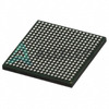

 OMAPL138BGWTMEPTexas InstrumentsIC MPU OMAP-L1X 345MHZ 361NFBGA
 OMAPL137DZKBA3Texas InstrumentsIC MPU OMAP-L1X 375MHZ 256BGA
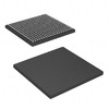
 OMAPL138AZWTTexas Instruments
 OMAPL138BGWTMEP
- Nath***rooks
- Jun 11, 2026
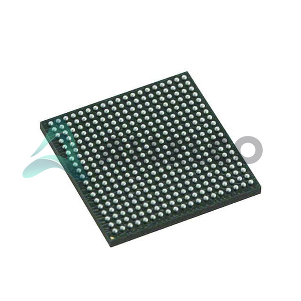
Image may be representation.
See specifications for product details.
See specifications for product details.
- EXPRESS OPTION
- Payment method
OMAPL138AZCE3 - Texas Instruments
- Manufacturer Part Number
- OMAPL138AZCE3
- Manufacturer
- Texas Instruments
- Allelco Part Number
- 98D-OMAPL138AZCE3
- Warranty
- 1 Year Allelco Warranty - Find out more
- Stock Status:
- 11,941 pcs available, New & Original
- Parts Description
- IC MPU OMAP-L1X 300MHZ 361NFBGA
- Package
- 361-NFBGA (13x13)
- Data sheet
-
OMAPL138AZCE3.pdf
Datasheets
OMAP-L138 Datasheet.pdfPCN Obsolescence/ EOL
Freon/Netra/SubArtic EOL 06/Oct/2015.pdf Freon/Netra/SubArtic EOL Update 4/Nov/2015.pdf
- RoHs Status
- ROHS3 Compliant
- Our certification
- In stock: 11941


